English
 Chinese



What’s the most expensive consumable in a wafer fab? It’s not the photoresist or the CMP slurry. It’s the wipe that nobody specs properly.
A process engineer at a 300mm fab in Hsinchu found this out the hard way. Yield dropped on one lot—random killer defects across the die, no pattern, no obvious cause. Two weeks tearing apart the lithography track, the etch chamber, the CMP tool. The culprit? A batch of wipes someone had brought into the wet bench area. These wipes were shedding a few hundred fibers per wipe—totally invisible—landing on 28nm gate oxide during a rinse step. One fiber, one dead die. Multiply that by a 25-wafer lot on a $12 million scanner, and the scrap bill hit hundreds of thousands.
That’s not an isolated incident. It plays out at fabs everywhere—Phoenix, Dresden, Samsung’s Pyeongtaek campus, the new TSMC plant in Kumamoto. The wipe is the cheapest item in your consumables budget. It’s also the one most likely to crater your yield if you pick the wrong one.
This guide is written for fab process engineers, cleanroom managers, and procurement teams who spec consumables for front-end wafer fabrication. Not packaging, not OSAT—FEOL, where a particle that doesn’t even show up on your metrology tool can kill a device worth $50,000 on the wafer.
Class 1 vs. Class 10: What the Standards Actually Mean for Your Wipe Choice
ISO 14644-1 defines cleanliness classes by maximum particle count per cubic meter. Class 1 allows just 10 particles ≥ 0.1µm per m³ and 2 particles ≥ 0.2µm per m³. Class 10 (ISO Class 2) is ten times more relaxed—100 particles ≥ 0.1µm per m³.
That gap matters a lot when you’re picking wipes. A wipe that passes in Class 10 can be a disaster in Class 1.
Most leading-edge logic fabs—5nm, 3nm—run Class 1 in lithography and diffusion. Memory fabs (NAND, DRAM) vary between Class 1 and Class 10 depending on the layer. Older fabs running 28nm or 65nm might sit at Class 100 (ISO Class 3) in general areas, but even those have specific steps—gate oxide formation, for example—where Class 1 is non-negotiable.
Your cleanroom team already knows these standards: IEST-RP-CC003 for garments and fabrics, IEST-RP-CC004 for wipe testing. Both reference Helmke drum testing (particles released under agitation) and liquid-borne particle count testing (extractables). If your wipe supplier can’t give you data against these standards, you’re flying blind.
Here’s what actually matters on the floor: the particle number on the spec sheet is tested under lab conditions. Your technicians fold the wipe, wet it, press it against surfaces, drag it across wafer carrier edges. Real-world particle release is almost always worse. A good supplier gives you both numbers—lab-tested and field-tested. The gap between those two numbers is where yield excursions live.
Particle Generation: Why the Spec Sheet Lies
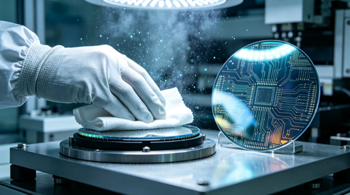
The Helmke drum test (IEST-RP-CC003.4, Method 20.2) tumbles wipes in a drum and counts the particles that come off. It’s the industry standard, and every supplier publishes results. But here’s the catch: the test simulates a wipe tumbling freely. Your technicians don’t tumble wipes.
They fold them, soak them, press them against surfaces, drag them across edges. The particle profile in actual use is different—and usually worse.
A wipe that scores ≤ 100 particles/m³ ≥ 0.5µm on Helmke might release 300–500 particles under real wet-bench wiping conditions. That doesn’t mean the test is broken—it means you need a safety margin. For Class 1 areas, spec a wipe that tests at Class 0.1 or better.
Particle generation also changes as the wipe ages. A fresh dry polyester wipe puts out fewer particles than one that’s been soaking in IPA for 20 minutes. Wet wipes behave differently from dry ones. Knit behaves differently from woven. Nonwoven behaves differently from both. Make sure the data your supplier gives you reflects how the wipe actually gets used in your fab—not just how it performs straight out of the bag.
And then there’s extractable particles. When you wet a wipe with your process solvent—IPA, acetone, DI water, whatever—particles dissolve out of the wipe material into the liquid. Those extractables end up on your wafer.
Liquid-borne particle counts (LBPC) per IEST-RP-CC004 tell you what’s coming out of the wipe in solution. For semiconductor work, you need extractable data specific to your process chemistry. Generic DI water testing isn’t enough.
ESD-Safe Wipes: The Silent Killer Nobody Budgets For
Electrostatic discharge kills wafers silently. Just 20 volts can punch through a thin-gate oxide. A person walking across a cleanroom floor generates 10,000–30,000 volts. The math doesn’t work in your favor.
In wafer handling areas—FOUP load ports, wafer sort, probe stations, any spot where bare wafers or die are exposed—wipes must be ESD-safe. That means either inherently antistatic materials (carbon fiber-loaded polyester, for example) or wipes treated with a durable antistatic agent that won’t leach out during use.
The difference between “antistatic” and “static dissipative” matters. Antistatic wipes stop charge from building up. Static dissipative wipes let charges bleed off in a controlled way. For semiconductor work, you want dissipative wipes with surface resistivity between 10⁶ and 10⁹ ohms/square—that’s the range specified in ANSI/ESD S20.20, the standard every fab uses.
Here’s where it goes wrong: ESD-safe wipes cost 2–3x more than standard cleanroom wipes. So someone in purchasing swaps in a “regular” cleanroom wipe, figures it’s close enough, and nobody catches it until a yield excursion forces a root cause investigation. By then, you’ve scrapped more wafer value than a decade of the right wipes would have cost.
One more thing: ESD properties degrade with use. A wipe rated at 10⁸ ohms/square fresh might climb to 10¹¹ after 30 minutes of wet wiping. If your process involves extended wiping sessions, test the wipe’s ESD performance in its used state—not just fresh from the bag.
Photoresist Compatibility and Wet Bench Cleaning
Photoresist gets everywhere in a fab. It’s on the wafer, the chuck, the edge bead removal ring, the track cup, the dispense nozzle—and if your wipes aren’t compatible, it’s on the wipe too. Residue from photoresist processing is some of the most stubborn contamination in semiconductor manufacturing. The wrong wipe material makes the problem worse, not better.
Polyester wipes are the standard pick for most fab applications, and they generally work fine with common photoresist solvents—PGMEA, EL, cyclohexanone, NMP. But “generally fine” isn’t the same as “tested and verified.” Some polyester wipes use binders or sizing agents that dissolve in strong solvents.
If you’re running NMP-based strippers or aggressive edge bead removal chemistries, you need to confirm the wipe material won’t degrade, shed, or release extractables when exposed to those specific chemicals.
Wet bench cleaning is where wipe selection gets critical. The wet bench is the last place your wafer touches before it goes into a furnace, oxidation tube, or deposition chamber. Any contamination introduced at the wet bench gets baked in—literally. Particles, ionic contaminants, organic residues—they all become permanent defects once they survive a 1,000°C thermal step.
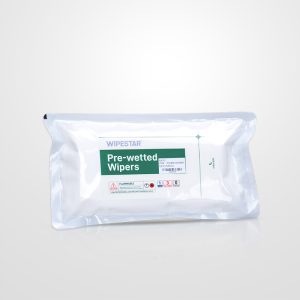
For wet bench work, you need two types: dry wipes for general surface cleaning (bench lips, tank edges, chemical delivery piping) and pre-wetted wipes for critical surface contact. Pre-wetted wipes eliminate the operator variability problem—someone always adds too much or too little solvent, and solvent purity depends on how the bottle was handled. Factory-sealed pre-wetted wipes with known solvent purity and saturation level remove that variable completely.
Ionic contamination from wipes is the topic that doesn’t get enough attention. Photoresist processing leaves ionic residues (Na⁺, K⁺, Cl⁻, SO₄²⁻) that migrate into gate oxide during thermal steps. Wipes that add ionic contamination to the wafer surface are actively doing harm. Your supplier needs to provide ionic extractable data—not just particle counts.
CMP Post-Clean: The Wipe Selection Nobody Talks About
CMP is one of the messiest steps in a modern fab. The slurry is a controlled disaster—colloidal silica or ceria particles, pH-adjusted surfactants, corrosion inhibitors—all designed to polish the wafer surface to sub-nanometer flatness. After CMP, the wafer is covered in slurry residue. The post-clean step removes that residue before the wafer moves on.
Post-clean typically involves a PVA brush scrub followed by a DI water rinse. But the wipes used to clean the CMP tool—the polishing pad carrier, the retaining ring, the slurry delivery lines, the wafer transfer mechanism—those are what prevent recontamination.
The slurry residue left behind is abrasive by design. If your wipe doesn’t trap and hold that residue, you’re just spreading it around. A wipe with poor particle-holding capacity—low absorbency, open weave, loose fiber structure—re-deposits slurry particles onto tool surfaces, where they’ll land on the next wafer.
Another CMP-specific concern is chemical compatibility. CMP slurries run alkaline (pH 10–11 for silica) or acidic (pH 3–4 for ceria). Your wipes need to hold up structurally and keep performing under those pH extremes. A wipe that works fine at neutral pH might fall apart in alkaline slurry, shedding fibers and binder particles that contaminate the tool.
For post-CMP work, we recommend a high-density polyester knit wipe with sealed edges and verified performance in both acidic and alkaline conditions. The wipe should have absorbency data at actual CMP slurry concentrations—not just generic DI water numbers. CMP post-clean areas typically run Class 10 or Class 100, so particle requirements are somewhat more relaxed than lithography, but still strict enough that a general-purpose industrial wipe won’t cut it.
Ionic Contamination: The Defect That Shows Up Six Months Later
If particle contamination is the obvious enemy, ionic contamination is the sneaky one. Particles kill die right away—you see them on the defect inspection tool, you know something’s wrong. Ions work differently.
They migrate through oxide layers under thermal stress and bias voltage, slowly degrading device performance over time. A wafer that passes final test can fail in the field six months later because sodium ions from a wipe migrated into the gate oxide during a 900°C anneal.
The semiconductor industry targets ionic contamination at the parts-per-billion level. For critical metals—sodium, potassium, calcium, iron, aluminum, zinc—the acceptable level in a wipe extract is typically < 1 ppm per individual ion, with total ionic contamination < 10 ppm. Some fabs, especially those running advanced nodes (< 7nm), specify < 0.1 ppm for sodium and potassium.
Testing follows IEST-RP-CC004.6, Method 012.2 (ion chromatography of wipe extracts). The wipe gets extracted in DI water at a controlled temperature and volume, then the extract goes through ion chromatography. Your supplier should provide this data per lot—not just a generic “meets spec” statement.
Lot-to-lot variation in ionic contamination is real. A wipe that tested clean in January might test dirty in March if the manufacturer changed a raw material or process parameter.
Metal ion contamination is especially critical for gate oxide integrity. Aluminum and iron ions, even at sub-ppm levels, create charge traps in thin SiO₂ layers. For fabs running high-κ metal gate processes, the wipe’s metal ion profile needs to be compatible with the specific metals in the gate stack—introducing trace amounts of a competing metal through a wipe can shift work function and threshold voltage.
Bottom line: particle counts alone don’t tell you if a wipe is safe for semiconductor use. You need ionic contamination data, extractable metal ion data, and ideally, performance data specific to your process chemistry. A wipe that’s “cleanroom grade” without semiconductor-specific ionic testing is a gamble. And in a fab, gambles cost real money.
Wipe Type Comparison: Side-by-Side
Semiconductor fabs typically use three main categories of wipes. The choice depends on your cleanroom class, the process step, and the chemical environment.
| Property | Polyester Knit (Sealed Edge) | Polyester/Cellulose Nonwoven | Continuous Filament Polyester |
|---|---|---|---|
| Cleanroom Class Suitability | Class 1 – Class 10 | Class 10 – Class 100 | Class 1 – Class 10 |
| Particle Generation (Helmke, ≥0.5µm) | ≤ 50 particles/m³ | 200–500 particles/m³ | ≤ 30 particles/m³ |
| Ionic Extractables | Low (< 5 ppm total) | Moderate (5–20 ppm) | Very Low (< 2 ppm) |
| ESD-Safe Versions Available | Yes (carbon-loaded) | Limited | Yes (inherently dissipative) |
| Chemical Compatibility | Excellent — IPA, acetone, PGMEA, DI water | Good — IPA, DI water; limited with strong solvents | Excellent — broad solvent resistance |
| Absorbency | Moderate (~3.5 mL/g) | High (~6–8 mL/g) | Low–Moderate (~2.5 mL/g) |
| Best For | Wet bench, general tool cleaning, photoresist areas | Equipment exterior, gowning area, spill cleanup | Critical wafer contact, CMP post-clean, lithography track |
| Relative Cost | $$ | $ | $$$ |
Quick note on cost: the cheapest wipe in that table runs about $0.08–$0.15 per wipe. The most expensive continuous filament polyester is $0.30–$0.60. That looks like a big gap until you compare it to one contaminated wafer at an advanced node.
One killed die at 3nm pays for a year’s supply of the best wipes on the market. Cost-per-wipe is the wrong metric. Cost-per-clean-wafer is what matters.
Most fabs run a two-tier strategy: premium continuous filament polyester for critical process areas (lithography, diffusion, CMP post-clean), and standard polyester knit for general cleanroom maintenance (equipment surfaces, bench tops, gowning areas). Some add a third tier—nonwoven wipes for corridors and change rooms—to control cost without compromising critical zones.
Whatever your approach, document the wipe spec in your cleanroom SOP and qualify the product before bringing it into the fab. “Qualification” means testing in your actual environment—your solvents, your wiping technique, your cleanroom conditions—not just trusting the supplier’s datasheet.
Who You’ll Work With at WIPESTAR
We supply cleaning consumables to semiconductor wafer fabrication plants where a single particle can destroy a $50,000 wafer. Our team understands Class 1/Class 10 cleanroom requirements and the strict contamination control standards of fab operations.

Zac — Customer Service
Zac focuses on professional and efficient customer service, dedicated to responding to inquiries quickly, handling orders smoothly, and providing reliable after-sales support.

Yunyun — ESD Project Manager
Yunyun is a dedicated ESD prevention professional with rich experience in static control technology research, application, and solution implementation for cleanroom environments.
Get Started with Semiconductor Wafer Fab Cleanroom Wipes
Whether you’re qualifying wipes for a new fab line, upgrading consumables for advanced node processing, or tracking down a yield excursion linked to contamination, we can help. Full documentation including COA, ionic analysis, and IEST-RP-CC004 compliance data.
- Cleanroom Wiper Selection Guide — Our full technical guide covering wipe materials, particle specs, and cleanroom class matching. Start here if you’re evaluating options.
- Browse All Wiping Cloths — Full product range with specs, certifications, and material data sheets for semiconductor-grade wipes.
- Request Technical Consultation — Need help matching a wipe to your specific process chemistry? Our team can provide ionic analysis and compatibility data for your fab.
Browse Full Wiping Cloths Range → Request a Custom Quote
Frequently Asked Questions