English
 Chinese



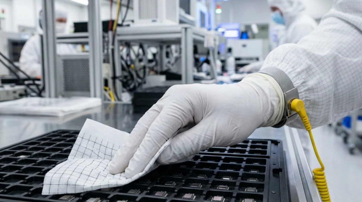
An OSAT (Outsourced Semiconductor Assembly and Test) facility in Penang was seeing a 2.3% yield loss on a QFN package line for a major automotive customer. The failure mode was intermittent open circuits on the wire bonds—sometimes the bond held, sometimes it didn’t. They’d optimized their bond parameters, replaced the capillary, and cleaned their bond pad surfaces. Yield improved 0.4%. Then a process engineer noticed that the wipes used to clean the lead frame feeders had a faint oily residue that wasn’t visible under normal lighting but showed up clearly under UV. The residue was a spin finish from the wipe’s polyester fiber manufacturing. It was transferring to the lead frame surface, contaminating the bond pad, and causing intermittent bond adhesion failures. One wipe specification change—switching to a low-extractable, ESD-safe cleanroom wipe with verified surface cleanliness—dropped the yield loss to 0.6%.
Semiconductor packaging and assembly is a different world from wafer fabrication. The cleanroom requirements are less stringent in terms of particle counts, but the contamination challenges are more diverse. You’re dealing with flux chemistry, die attach adhesives, molding compounds, and lead frame metallurgy—all of which interact with cleaning consumables in ways that don’t show up in a wafer fab environment. Most of the cleanroom wipe guides on the market focus on front-end fabrication. This one focuses on the back end—where the chips get packaged, tested, and shipped.
Why Semiconductor Packaging Has Different Wipe Requirements Than Wafer Fab
In wafer fabrication, the primary contamination concern is particles on a silicon surface. A single sub-micron particle on a gate oxide can kill a transistor. The wipe specifications are accordingly extreme—ISO Class 5, sub-100 particles per cm², laser-sealed edges, the works.
In packaging, the particle spec is more forgiving (you’re not printing transistors on a lead frame), but the contamination chemistry is far more complex. Flux residues from solder reflow are ionic and corrosive—they cause electromigration and corrosion failures in the field. Die attach adhesives outgas during cure and leave films on adjacent surfaces. Molding compound flash is thermoset plastic that bonds permanently if not cleaned within hours. Lead frame plating chemistries (nickel-palladium-gold, tin) are sensitive to organic contamination that affects solderability.
The wipe material that works in a wafer fab—typically 100% polyester, knit, laser-sealed—may not be optimal for packaging applications. You might need different materials for different process stages. And the ESD requirements are different: wafer fab wipes need to be antistatic (prevent charge generation), while packaging wipes often need to be dissipative (controlled charge dissipation) to protect devices that are no longer on the wafer and are more susceptible to CDM (charged device model) damage.
We’ve published a guide on cleanroom wipes for semiconductor wafer fabrication that covers the front-end requirements. Here, we focus on the back-end—packaging, assembly, and test.
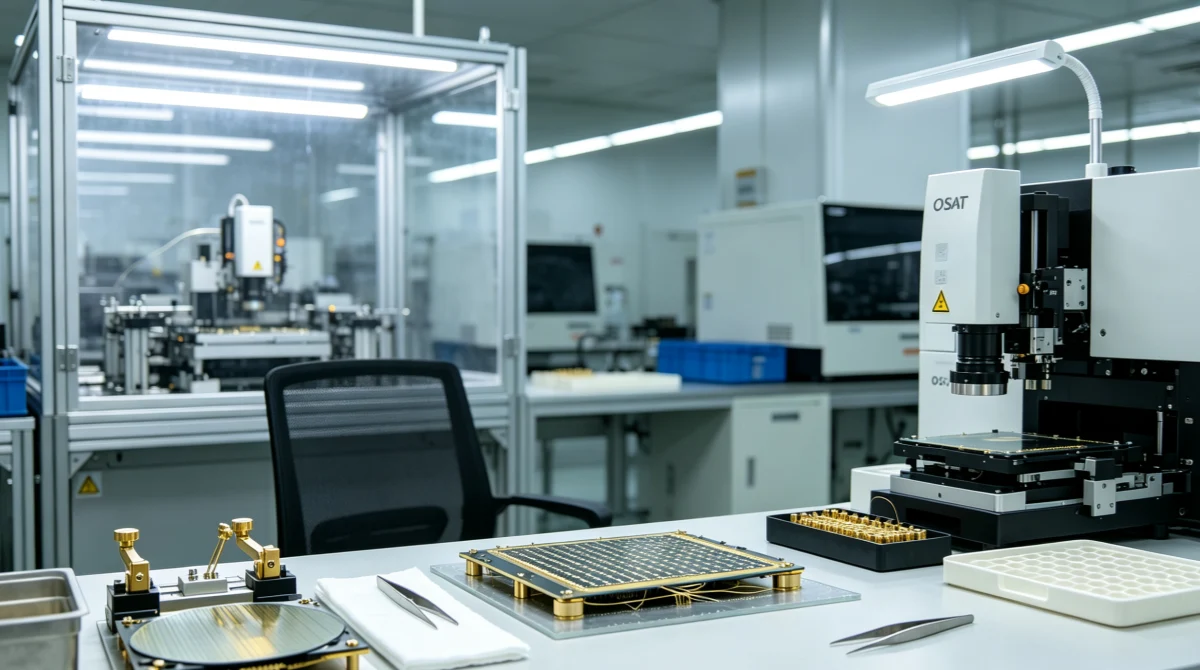
Wipe Selection by Process Stage: Die Attach, Wire Bonding, Molding, Plating, Test
Die Attach
Die attach adhesive (typically silver-filled epoxy or sintered paste) is dispensed onto the lead frame or substrate, and the die is placed on top. Wipes are used to clean dispensing needle tips, adhesive overflow from the die edge, and substrate surfaces before die placement. The adhesive is thermosetting—once it cures, it’s permanent. Wipes must absorb uncured adhesive without leaving fibers on the substrate surface. Low-lint polyester/cellulose blends work well here.
Wire Bonding
This is the most wipe-sensitive stage in packaging. Gold or aluminum wire bonds connect the die pads to the lead frame. The bond surface must be scrupulously clean—any organic contamination (fingerprints, flux residue, spin finish from a wipe) weakens the bond adhesion and causes field failures. Wipe requirements: ultra-low extractables, no processing aids or lubricants on the fiber, and ESD-safe construction. The wipe itself must not be the contamination source.
Molding
Epoxy mold compound encapsulates the die and wire bonds. Flash—thin excess mold compound that squeezes out at the mold parting line—must be cleaned before it cures. Once cured, flash removal requires mechanical abrasion or laser ablation, which is expensive and risky. Wipes used for flash cleanup must absorb uncured epoxy quickly and not react with the mold compound chemistry. Chemical compatibility with anhydride-cured and novolac-cured epoxy systems is essential.
Plating
Lead frame plating—typically NiPdAu (nickel-palladium-gold) or pure tin—requires clean surfaces for good plating adhesion. Wipes used on plating fixtures and racks must not leave organic residues that cause plating voids or adhesion failures. Chemical resistance to plating chemistries (sulfamate nickel, acid gold, methanesulfonic acid tin) is required.
Test and Final Inspection
Handler fixtures and contact pins accumulate flux residue, mold compound dust, and lead frame debris during production. Wipes used for handler maintenance need to remove these residues without damaging the precision contact pins. Chemical compatibility with IPA and the ability to remove ionic flux residues are the priorities here.
Flux Residue Management: The Silent Yield Killer
Flux is used in solder reflow processes (die attach with solder preforms, BGA ball attach, wave solder for through-hole components). After reflow, flux residue remains on the substrate surface. This residue is ionic—it conducts electricity under humidity and causes electromigration, corrosion, and leakage current failures.
The problem: flux residue isn’t always visible. No-clean fluxes are designed to leave minimal residue, but “minimal” isn’t “zero.” Under humid conditions or extended field operation, even small amounts of ionic residue cause failures. Your wipes need to remove flux residue—not just spread it around.
Effective flux removal requires either:
- A pre-wetted wipe with saponifier or flux remover chemistry (IPA alone doesn’t fully dissolve rosin-based flux residues)
- A dry wipe followed by a spray-on flux remover, then a second dry wipe to remove dissolved residue
- A wipe material with enough surface energy to mechanically lift flux residue (microfiber or textured non-woven)
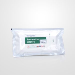
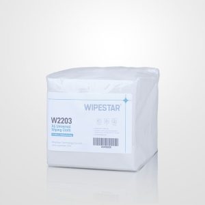
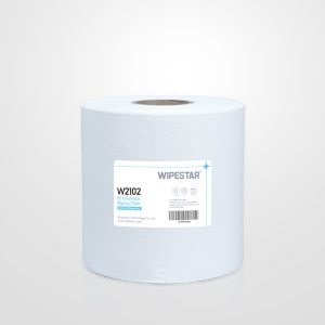
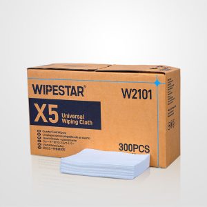
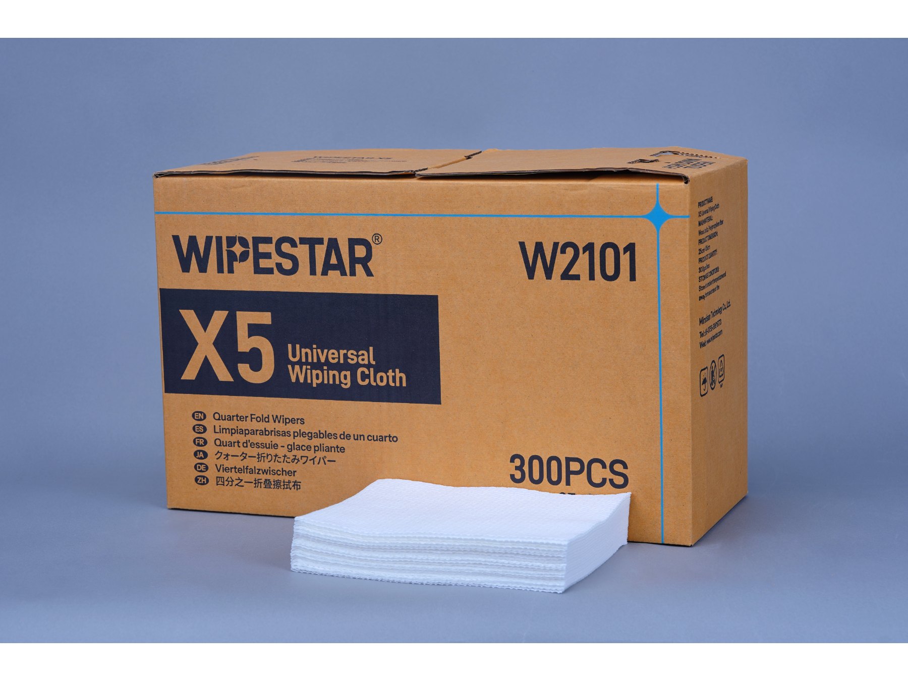
Our pre-wetted wipes are available in IPA and specialty solvent formulations suitable for flux residue removal. For dry wipe applications, our wiping cloths range includes low-extractable products specifically tested for semiconductor packaging environments.
ESD Safety: Why Your Wipe Must Be Dissipative, Not Just Antistatic
In wafer fab, the primary ESD concern is preventing charge buildup on the wipe itself (antistatic). In packaging, the concern shifts: devices are now individual units—dies on lead frames, packaged ICs in trays—and they’re susceptible to CDM (charged device model) damage. A device that charges up and then discharges through a bond pad can destroy the gate oxide without any visible damage.
Your wipe needs to be dissipative (surface resistivity 10⁶ to 10⁹ ohms/square), not just antistatic (which simply means it doesn’t generate static). A dissipative wipe allows controlled charge equalization between the wipe and the device surface, preventing the rapid discharge that causes CDM damage. An antistatic wipe that’s insulative (above 10⁹ ohms/square) can actually make CDM worse by allowing charge to build up on the device without a discharge path.
Verify the surface resistivity specification of your wipes before using them near unpackaged devices. Our ESD-safe cleanroom wipes are tested per ANSI/ESD STM11.11 and verified to be in the dissipative range. Request the surface resistivity test report from our team.
Lead Frame and Substrate Cleaning: Surface Energy and Wetting
Lead frames and BGA substrates have specific surface energy requirements for successful die attach, wire bonding, and soldering. A surface contaminated with organic residue has lower surface energy—the adhesive or solder doesn’t wet properly, and the joint fails.
Your wipe must clean the surface without leaving a residue that lowers surface energy. This is where the “cleanroom grade” label isn’t enough. A wipe that’s excellent for particle removal in a wafer fab might leave a thin organic film (from spin finish, edge seal adhesive, or packaging material) that reduces surface energy on a lead frame. The result: intermittent die attach voids or wire bond non-sticks that show up as yield loss.
For lead frame and substrate cleaning, specify wipes with verified low extractable residue (below 50 ppm total extractables per wipe, tested by gravimetric method) and no adhesive in the construction. Request surface energy test data (dyne/cm) for the wipe material itself—if the wipe’s surface energy is lower than your target surface cleanliness, it can’t clean effectively.
Mold Compound Flash Cleanup: Chemical Compatibility Matters
Epoxy mold compounds are thermoset plastics. Once cured, they’re permanent. But during the molding process, flash (excess compound) remains soft for a limited time window. Wipes used for flash cleanup must absorb the uncured compound before it cross-links.
The challenge: uncured mold compound contains anhydride hardeners, epoxy resins, and various fillers (silica, carbon black). These chemicals are irritants and sensitizers. Your wipe must absorb them without degrading or releasing the absorbed compounds back to the operator’s skin. Nitrile gloves are standard in molding areas, but the wipe should not require bare-hand handling at any point.
Chemical compatibility with your specific mold compound system is essential. Test the wipe with your actual molding compound—don’t assume compatibility based on the base fiber material. The hardener chemistry (anhydride vs. phenolic vs. novolac) affects wipe compatibility differently.
Documentation for OSAT Quality Systems
OSAT facilities operate under quality systems driven by their automotive, industrial, and consumer electronics customers. The documentation requirements for consumables are typically specified in the customer’s quality agreement, not just by the OSAT’s internal system. Here’s what’s typically required:
- Certificate of Analysis (COA) — Particle counts, extractable residue, surface resistivity (for ESD products), and dimensional verification per lot.
- ESD Test Report — Surface resistivity per ANSI/ESD STM11.11 or equivalent. For dissipative wipes, the report should confirm the 10⁶–10⁹ ohms/square range.
- Raw Material Traceability — Base fiber composition, all processing aids, edge seal materials, and packaging materials. Automotive customers (IATF 16949) require full material disclosure.
- Change Notification Agreement — Written commitment to notify before any change to raw materials, manufacturing process, or sterilization method. Automotive and industrial customers treat this as a contractual requirement.
- ROHS and REACH Compliance — Declaration of compliance with EU RoHS (2011/65/EU) and REACH (EC 1907/2006) regulations. Required for any facility serving European end markets.
The Problems We See in Packaging Houses
- Using wafer-fab-spec wipes for packaging applications — The particle spec is overkill, but the extractable spec may be insufficient. Wafer-fab wipes are optimized for particle control, not for organic contamination control. Packaging applications need the opposite priority.
- Antistatic wipes near unpackaged devices — An antistatic wipe that’s insulative (above 10⁹ ohms/square) can cause CDM damage to bare dies and wire-bonded devices. Verify dissipative surface resistivity before using wipes near unpackaged devices.
- Spin finish contamination on bond pads — The most common cause of intermittent wire bond failures. The wipe’s polyester fiber carries trace spin finish from the fiber manufacturing process. Switching to a low-extractable, semiconductor-grade wipe eliminates the issue.
- No ESD test data on file — Your customer’s quality agreement requires ESD-safe consumables, but your wipe supplier’s COA doesn’t include surface resistivity testing. This is a customer audit finding that’s easy to prevent.
- Adhesive-bonded wipes in molding areas — Uncured mold compound solvents dissolve adhesive bonds. Wipe delamination in a molding area introduces particles and adhesive residue to the device. Specify ultrasonic-sealed or heat-sealed edges.
Who You’ll Work With at WIPESTAR
Our team has worked with semiconductor packaging and OSAT facilities across Asia—including major operations in Malaysia, China, Taiwan, and the Philippines. We understand the quality system requirements of automotive, industrial, and consumer electronics customers.

Ethan — Sales Director
Ethan has over 20 years in the cleanroom consumables industry, including direct experience with semiconductor packaging operations. He leads our OSAT accounts—facilities that need ESD-safe products, automotive-grade documentation, and change notification agreements.

Yunyun — ESD Project Manager
Yunyun is our ESD Project Manager, specializing in electrostatic discharge protection for semiconductor and electronics manufacturing. She ensures the ESD-safe wipes we deliver to OSAT facilities meet the dissipative surface resistivity requirements (10⁶–10⁹ ohms/square) that CDM-sensitive devices demand.

Vicky — Foreign Trade Sales Supervisor
Vicky manages our semiconductor packaging accounts in Southeast Asia and other regions. She has worked with OSAT facilities navigating customer quality audits and ensures every order includes ESD test reports, RoHS/REACH declarations, and change notification agreements.
Get Started with Semiconductor Packaging Cleanroom Wipes
Whether you’re qualifying wipes for a new packaging line, upgrading your ESD-safe consumables for an automotive customer audit, or solving a wire bond yield issue, we can help. Full documentation packages including COA, ESD test reports, RoHS/REACH declarations, and change notification agreements.
Browse our wiping cloths range or contact our technical team to discuss your packaging facility’s specific requirements.
Frequently Asked Questions About Cleanroom Wipes for Semiconductor Packaging
Request a Quote for Semiconductor Packaging Cleanroom Wipes
We supply ESD-safe cleanroom wipes from our ISO 9001:2015 certified factory with full packaging documentation—COA, ESD test reports, RoHS/REACH declarations, and change notification agreements. Custom sizing and private labeling available. Fast shipping to OSAT facilities globally.