English
 Chinese

A 300mm wafer fab in Dalian contacted us after their yield dropped 1.2% in a single quarter. The root cause? A wipe their procurement team had been buying for three years—the same product, same spec sheet, same supplier—had a subtle shift in particle generation. The CoA said it passed. Their KLA inspection tool said it didn’t. The delta was 47 particles per wafer at ≥0.05μm. Enough to kill yield on their 7nm node.
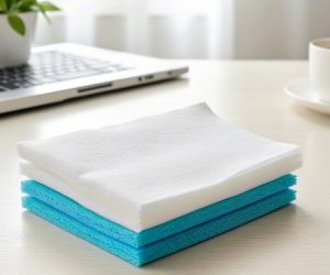
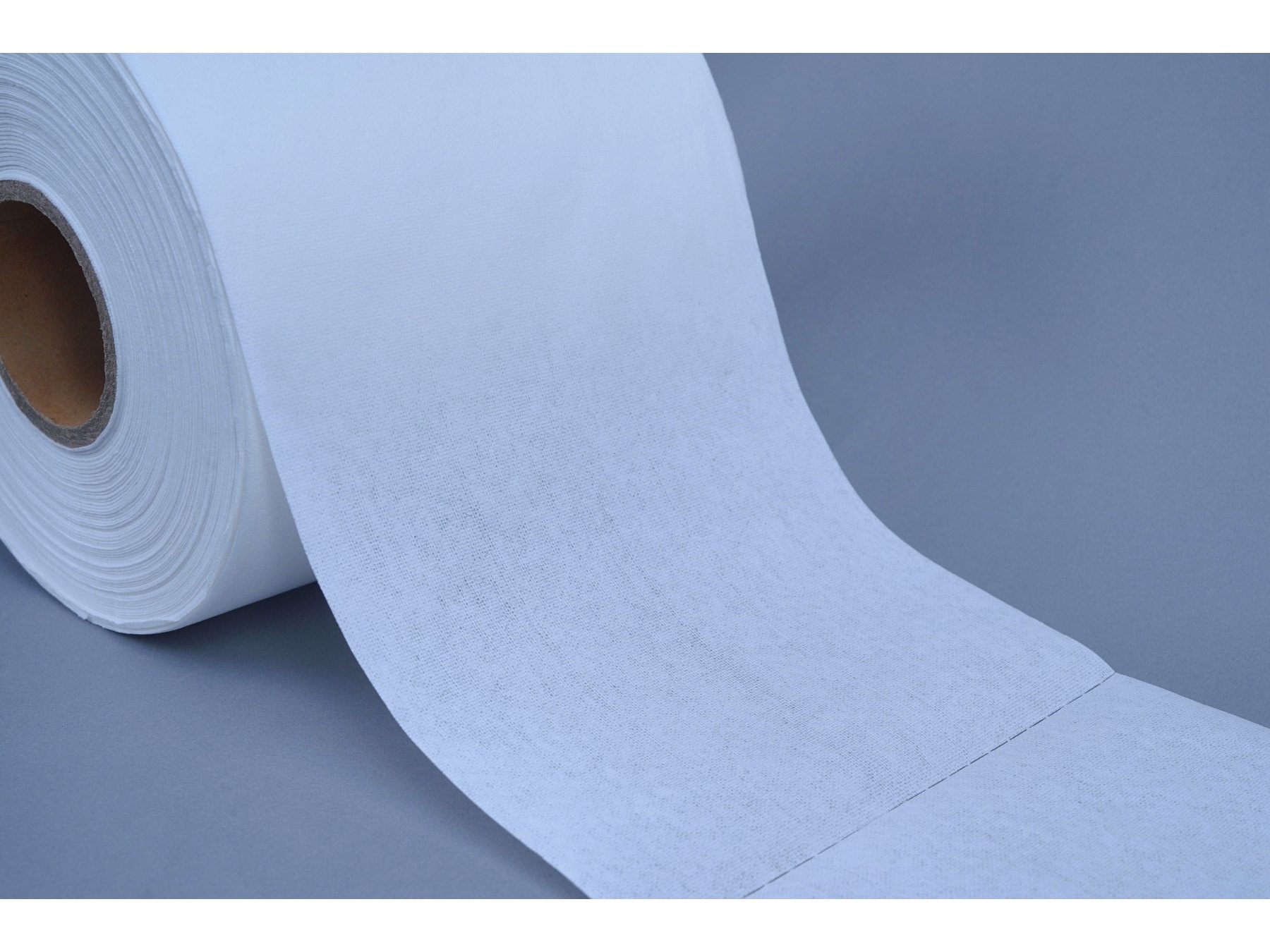
We supply cleanroom consumables to semiconductor fabs, OSAT facilities, and equipment OEMs across Asia. This guide covers what we’ve learned about matching cleanroom wipes to wafer fabrication environments—where the specs are tighter than any other industry, and where “close enough” is never close enough.
Why Semiconductor Fabs Demand a Different Class of Cleanroom Wipe
In most cleanroom environments, a particle at 0.5μm is the threshold of concern. In a wafer fab running 7nm or 5nm process nodes, that threshold drops to 0.03μm or below. The wipe that passed every spec sheet in your pharmaceutical or flat-panel display application is generating particles you can’t even measure with standard optical counters—but your e-beam inspection tool sees every one of them.
This isn’t a matter of buying “better” wipes. It’s a fundamentally different specification framework:
- Particle counts are measured at ≥0.03μm, not ≥0.5μm — Standard IEST-RP-CC004 testing uses 0.5μm as the lower threshold. Semiconductor fabs need LPC (Laser Particle Counter) data at 0.03μm or below. If your supplier can’t provide this data, their wipes are unqualified for your fab regardless of what the spec sheet claims.
- Extractable metals matter — A wipe that leaves behind sodium, potassium, or trace metal ions on a wafer surface can cause gate oxide defects and junction leakage. Your wipe’s extractable metal profile must be documented per SEMI standards.
- ESD generation is a yield issue — Static charge on a wipe attracts particles to the wafer surface and can damage sensitive gate structures. Anti-static properties aren’t a nice-to-have; they’re a line item in your contamination control strategy.
If you’re sourcing cleanroom wipes for wafer fab applications, the qualification process is longer and the documentation requirements are heavier than any other industry we serve. But the payoff is measurable in yield points.
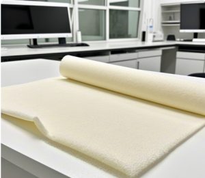
ISO Class 1–3: What Wipe Specifications Actually Mean at This Level
Most cleanroom wipe suppliers test and certify their products to ISO Class 5 (Class 100) standards. That’s fine for flat-panel displays, medical devices, and most pharmaceutical applications. It’s completely inadequate for wafer fabrication.
Particle Specifications at the Sub-Micron Level
In an ISO Class 1 environment, the allowable particle count is 10 particles per cubic meter at ≥0.1μm. Your cleanroom wipe must not introduce particles that push you above this threshold during normal use. Here’s what that means in practice:
- Wipe particle generation must be tested at ≥0.03μm using a condensation nucleus counter (CNC) or ultrafine LPC, not just a standard optical particle counter.
- Lot-level particle data is essential. Averages across production runs hide the outlier lots that contaminate your process.
- Testing must simulate actual use conditions—wet wiping, dry wiping, and wipe-down under laminar airflow—not just bag-count testing on pristine samples.
Extractable Metal Specifications
SEMIF47 and SEMIF21 standards define acceptable extractable metal levels for materials entering semiconductor cleanrooms. Your wipe supplier should provide ICP-MS (Inductively Coupled Plasma Mass Spectrometry) data showing extractable levels for:
- Sodium (Na), Potassium (K), Calcium (Ca) — alkali metals that cause mobile ion contamination
- Iron (Fe), Copper (Cu), Zinc (Zn) — transition metals that cause junction leakage
- Aluminum (Al) — causes gate oxide integrity failures
Typical acceptance limits are below 1 ppb (parts per billion) per element for critical process wipes. If your supplier’s CoA shows extractables in ppm (parts per million), that product isn’t fab-grade.
ESD Safety: The Hidden Killer in Wafer Fabs
Electrostatic discharge is the contamination source nobody sees until yield data screams. A wipe that generates even 50V of static charge during use can:
- Attract airborne particles from the surrounding environment onto the wafer surface — particles that would otherwise have been captured by your HEPA/ULPA filtration.
- Damage thin gate oxides in advanced CMOS devices — gate oxide breakdown voltages on 5nm nodes are below 2V. A 50V static event from a wipe is 25× the damage threshold.
- Cause charge-induced pattern shifting in e-beam lithography — if you’re running EUV or e-beam process steps, static from consumables near the tool can deflect the beam.
This is why we assign a dedicated ESD Project Manager to every semiconductor account. Yunyun works directly with your contamination control team to test wipe surface resistivity, charge decay time, and triboelectric charge generation under your specific cleanroom conditions. Generic “anti-static” claims on a spec sheet don’t tell you enough—you need testing under your airflow, your humidity, and your wipe-down protocol.
Surface resistivity for fab-grade wipes should fall in the dissipative range: 10⁶ to 10⁹ ohms/square. Below 10⁶, the wipe becomes conductive and could create a shorting hazard near powered equipment. Above 10⁹, the anti-static property is negligible.
Chemical Compatibility with Fab Process Chemicals
Wafer fabs use aggressive chemicals that would destroy standard cleanroom wipes. Your wipe must maintain physical integrity and particle performance when exposed to:
Common Fab Solvents and Their Wipe Requirements
| Chemical | Application | Wipe Requirement |
|---|---|---|
| IPA (Isopropyl Alcohol) | General surface cleaning, wafer edge rinse | Standard polyester or polyester/cellulose blend |
| Acetone | Photoresist removal, heavy organic cleaning | 100% polyester with high chemical resistance |
| PGME / PGMEA | Solvent-based developers and strippers | Polyester with verified low extractables in glycol ethers |
| Dilute HF | Native oxide removal, wet bench cleaning | Polypropylene or PTFE — polyester degrades in HF |
| SC-1 / SC-2 | RCA clean solutions (H₂O₂-based) | Polyester or polypropylene — verify H₂O₂ compatibility |
One mistake we see repeatedly: fabs use the same polyester wipe for IPA cleaning and HF bench wiping. Polyester dissolves slowly in hydrofluoric acid, releasing fibers and extractable organics directly onto the wafer. If you have HF process steps, you need a dedicated polypropylene or PTFE wipe for those stations. Mark them with a different color packaging to prevent cross-contamination.
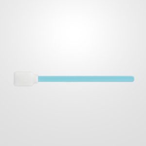
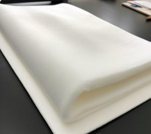
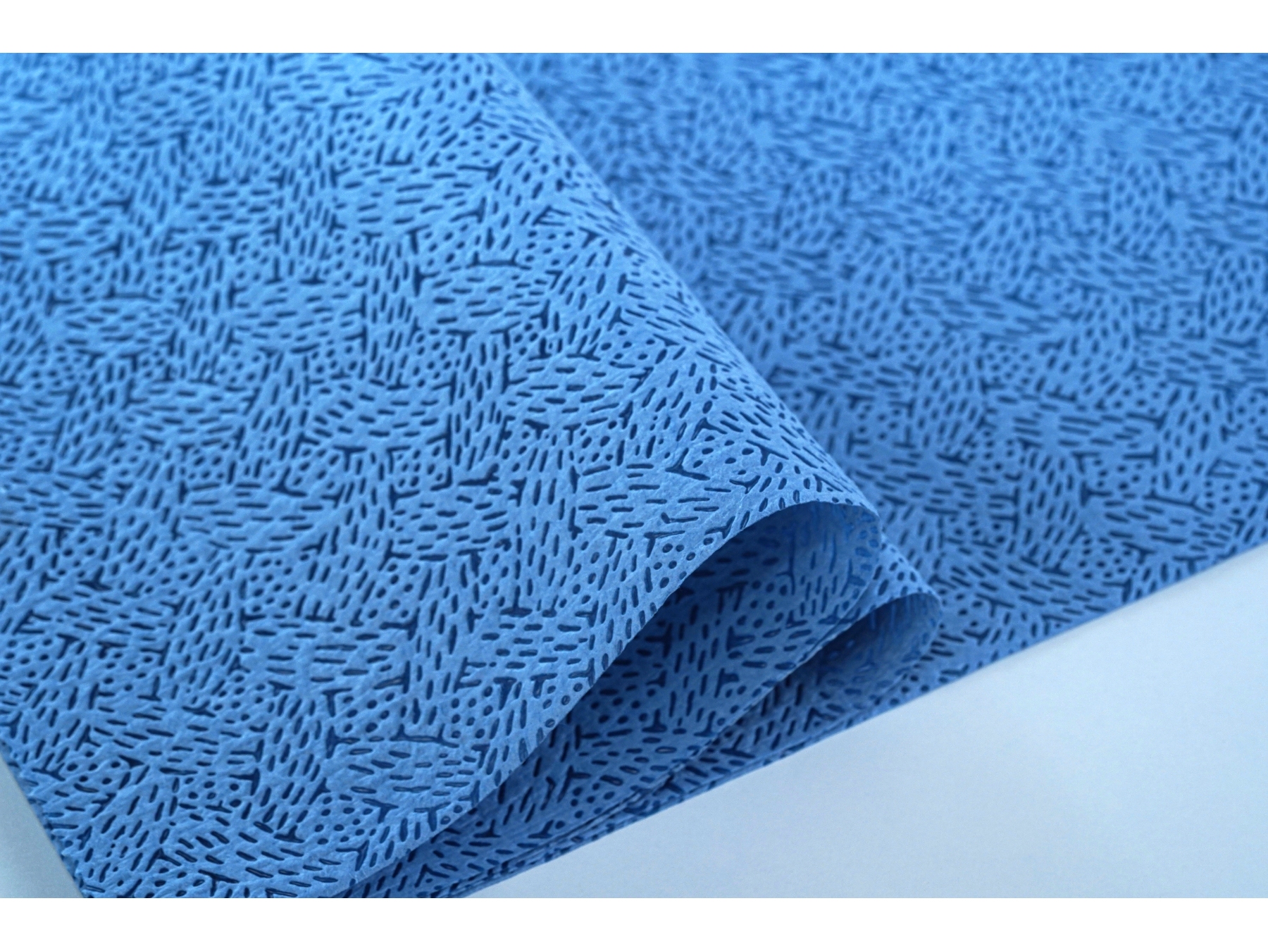
Edge Construction and Particle Generation at Sub-Micron Levels
In pharmaceutical or display cleanrooms, the difference between a cut-edge and a laser-sealed wipe matters. In semiconductor fabs, it’s the difference between passing and failing an inspection. Here’s why:
At the sub-micron level, a single fiber from a wipe edge is visible on a wafer inspection tool. That fiber becomes a defect site that can cause:
- Particle-induced pattern defects in lithography — a fiber on the reticle or wafer surface distorts the projected image.
- Etch residue trapping — fibers trap etch byproducts and release them during subsequent process steps.
- Probe card contamination — for test and sort operations, fibers on probe tips cause contact failures and false binning.
For wafer fab applications, ultrasonic-sealed edges are the minimum. Some fabs specify laser-sealed for general cleaning and reserve ultrasonic-sealed for critical process tools. The cost difference is real—ultrasonic-sealed wipes cost 30–50% more than heat-sealed—but so is the particle reduction. We’ve documented 80–90% fewer fiber defects on wafer inspection when fabs upgraded from heat-sealed to ultrasonic-sealed edges.
Wet vs. Dry Cleanroom Wipes: When to Use Each
The wet-vs-dry decision in a wafer fab isn’t just preference—it’s process-dependent and contamination-dependent.
Use Dry Wipes When:
- Wiping down tool exteriors, load ports, and FOUP/reticle pod surfaces where no liquid residue is acceptable.
- Performing final wipe-down before tool qualification after preventive maintenance.
- Working near exposed wafer surfaces where liquid carryover could cause watermark defects.
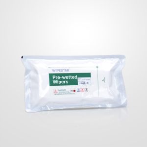
Use Pre-Wetted Wipes When:
- Removing organic residues (photoresist, flux, fingerprints) that require solvent action.
- Wiping down wet bench interiors and chemical delivery surfaces.
- Performing IPA wipe-down of wafer chucks and electrostatic chuck surfaces where a controlled amount of solvent aids particle removal.
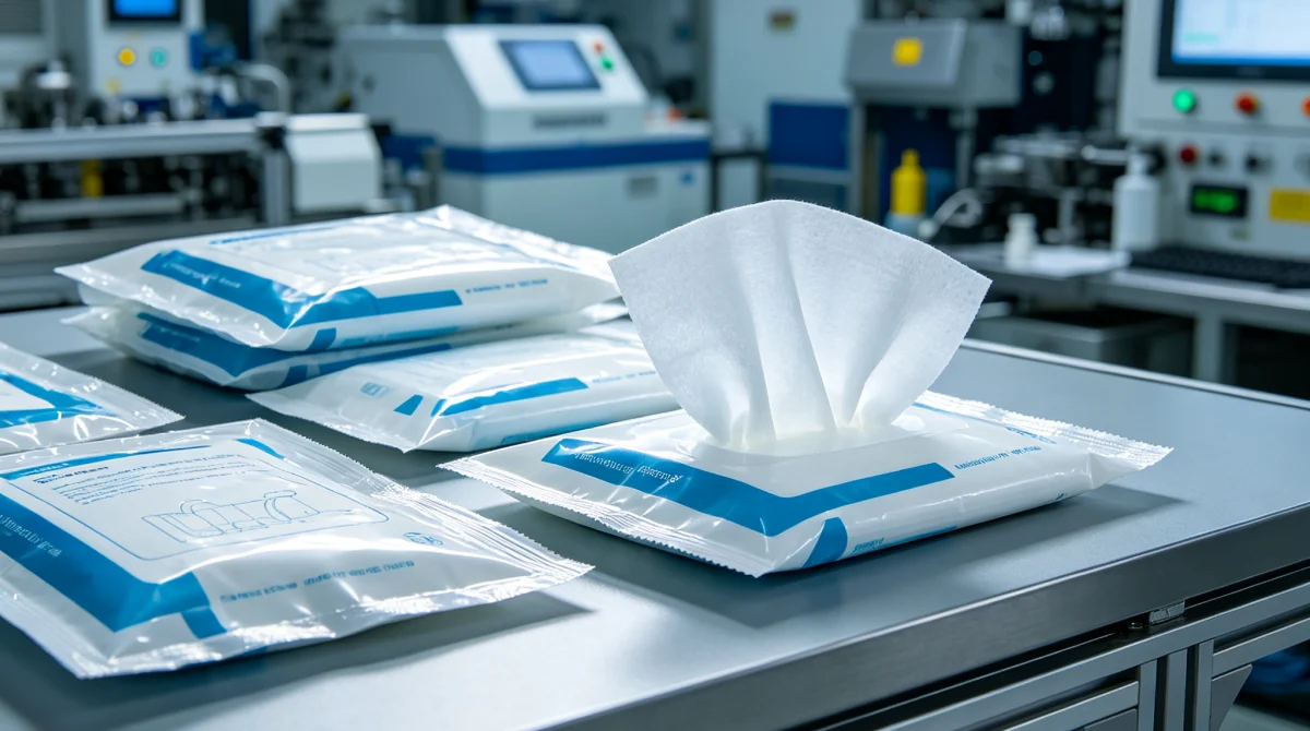
Pre-wetted wipes should be saturated with a controlled amount of solvent—typically 60–70% IPA in DI water—and sealed in individual pouches to prevent solvent evaporation and recontamination. Open-bucket dipping of dry wipes into solvent containers is a contamination source, not a cleaning method. We’ve seen fabs eliminate an entire class of particle defects simply by switching from bucket-dipped to individually packaged pre-wetted wipes.
Packaging and Handling Protocols for Fab-Grade Wipes
Even the best cleanroom wipe becomes a contamination source if the packaging and handling protocol is wrong. For semiconductor fabs:
- Double-bag in cleanroom-grade packaging — Outer bag for transport protection, inner bag is the cleanroom transfer pouch. Both bags must be compatible with your pass-through or airlock sterilization method if required.
- Individual pouch packaging for pre-wetted wipes — Each wipe in its own sealed pouch. No bulk packaging for fab-grade applications.
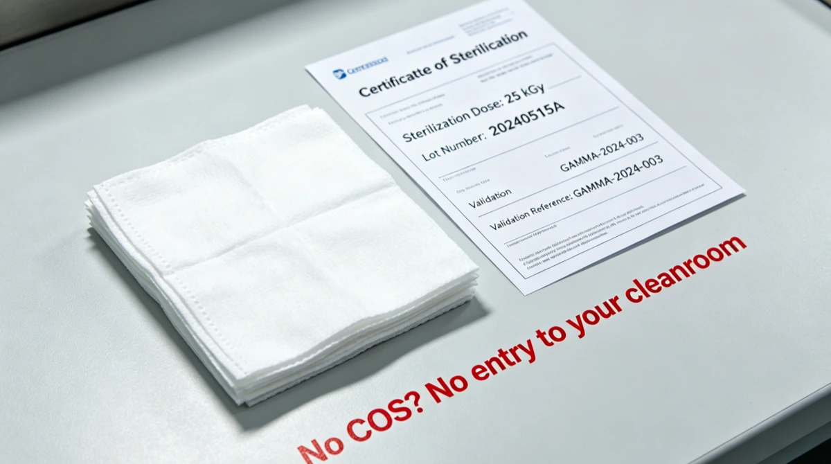
- Lot-level labeling — Each package must show lot number, manufacturing date, particle count data reference, and extractable metal data reference. If your receiving team can’t trace the wipe back to its CoA, the wipe can’t enter the fab.
- Storage in climate-controlled areas — Temperature and humidity affect wipe particle performance. Store in clean, dry areas below 25°C and below 50% RH. FIFO rotation is mandatory.
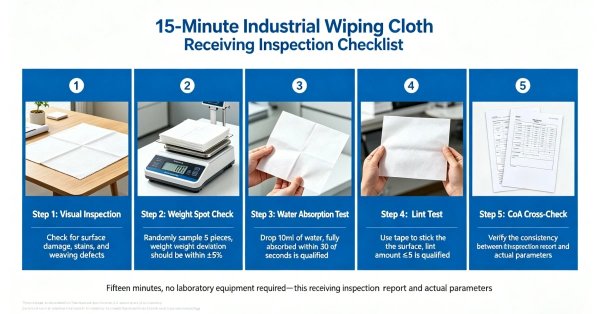
How to Qualify a Cleanroom Wipe Supplier for Semiconductor Applications
Semiconductor wipe qualification is a multi-month project, not a single purchase order. Here’s the framework we walk through with fab customers:
Phase 1: Specification Review
Map your process requirements against the supplier’s product specifications. Verify particle data at ≥0.03μm, extractable metal data per SEMI standards, ESD surface resistivity, and chemical compatibility with your process chemistries. If the supplier can’t provide any of these, stop here.
Phase 2: Engineering Samples
Request engineering sample lots with full documentation. Test in your cleanroom environment using your standard wipe-down protocol. Run particle counts on your surfaces before and after wipe-down. Compare against your current product baseline.
Phase 3: Pilot Production
Place a pilot production order and track yield impact across at least two wafer lots. Correlate your e-beam inspection data and KLA defect maps with the wipe lot number. This is where real performance shows up—not in a lab test, but in your production yield.
Phase 4: Ongoing Monitoring
Set up lot-level incoming inspection: verify CoA data matches physical product, run spot particle checks, and maintain documentation in a retrievable system. Schedule quarterly supplier performance reviews against your yield data.
We’ve supported semiconductor fab qualifications across TSMC, Samsung, SMIC, and Intel supply chains. If you need a supplier who understands fab-grade documentation from the start, browse our cleanroom wipe range or contact our semiconductor team directly.
Specialists You’ll Work With at WIPESTAR
Semiconductor accounts get a dedicated team that understands fab contamination—not generalists who sell the same wipe to every industry.

Ethan — Sales Director
20+ years in cleanroom consumables. Ethan has worked with semiconductor fabs since the 200mm era and understands how process node shrinks change consumable requirements. He leads our semiconductor account strategy and handles the kind of multi-site, multi-year supply agreements that fabs need.

Yunyun — ESD Project Manager
Static charge is a yield issue in every wafer fab. Yunyun runs ESD qualification testing for every semiconductor wipe we supply—surface resistivity, charge decay rate, and triboelectric charge generation under fab-specific conditions. She works directly with your contamination control engineers to match wipe ESD properties to your process requirements.

Carolina — Product Specialist
Carolina works on the factory floor with our production team, monitoring raw material consistency and process control. For semiconductor accounts, she manages the tighter lot-release criteria that fabs demand—every lot ships with particle data at ≥0.03μm, ICP-MS extractable metal reports, and ESD test certificates. She catches the lot-to-lot variation before it reaches your fab.
See the full team: WIPESTAR Team Page →
Frequently Asked Questions About Cleanroom Wipes for Semiconductor Wafer Fabrication
Request Fab-Grade Cleanroom Wipe Samples
We supply semiconductor-grade cleanroom wipes direct from our factory—full SEMI-standard documentation, ICP-MS extractable metal reports, ESD test certificates, and lot-level particle data at ≥0.03μm. ISO 9001:2015 certified production. Free engineering samples for qualified semiconductor facilities.
Browse our cleanroom wipe range →