English
 Chinese



Last year we got a call from a contract manufacturer in Suzhou. They’d been chasing intermittent solder bridges on a batch of IoT modules—about 2% failure rate at AOI. Doesn’t sound like much until you’re running 50,000 units a week. They’d reflowed the reflow profile, checked paste volume, swapped out the stencil tension test. Three weeks of head-scratching. We went on-site, took one look at the wipe they were using for stencil cleaning, and knew immediately. The fibers were too coarse. Every pass left microscopic filament residue on the stencil—nearly invisible to the naked eye, but more than enough to bridge between fine-pitch pads.
Switched to the right polyester knit cleanroom wipe. Defect rate dropped below 0.1% within three days. Their procurement manager said something that stuck with me: “I thought a wipe was just a wipe.”
This article is for anyone who still thinks that way. The cost of choosing the wrong cleanroom wipe goes far beyond how many sheets you burn through—it cascades into yield loss, rework costs, and customer complaints you never saw coming.
Why Cleanroom Wipe Selection Matters More Than You Think
I’ve walked through factories that spent hundreds of thousands on SMT placement equipment, reflow ovens, AOI systems—and then bought the cheapest wipe they could find for stencil cleaning. “It works, that’s all we need.” Except it doesn’t work. Not really.
Electronics manufacturing has almost zero tolerance for contamination. A single 5-micron particle on a wafer surface can kill a die. One stray fiber on a PCB pad before solder paste application can cause an open circuit. An invisible ESD discharge hitting a MOSFET—nothing visible on the component, just a latent defect waiting to surface as a field failure six months down the road.
These aren’t theoretical risks. They happen every day on SMT lines, in semiconductor fabs, in precision electronics assembly cleanrooms. And they almost always trace back to one decision nobody spent enough time on: which cleanroom wipe your operators grab a few thousand times per shift.
The tricky part is that wipe selection isn’t straightforward. There are a dozen materials, multiple edge treatments, cleanliness grades spanning ISO 3 through ISO 8, plus ESD properties, pre-wetting options, ion extractables—specs that most procurement teams never even ask about. A wipe that performs brilliantly for semiconductor wafer fabrication might be completely wrong for a PCB rework station. One that works fine for general equipment wipe-down could be a disaster in an ESD-protected area.
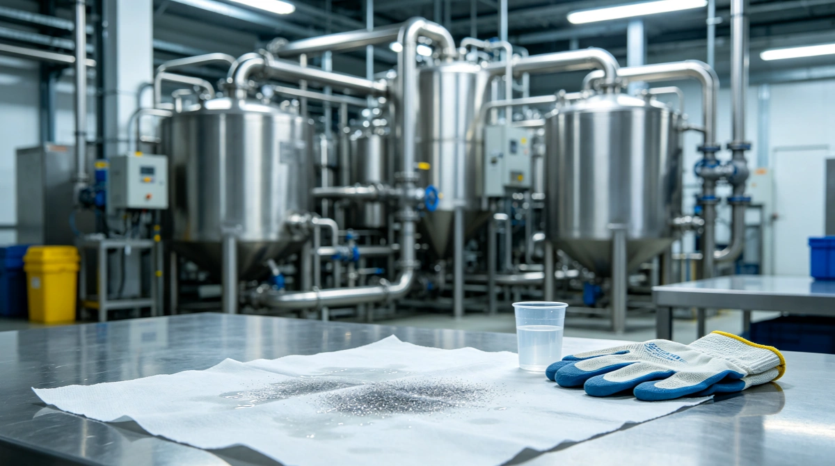
Three Main Materials: Polyester, Microfiber, and Non-Woven—How to Choose
Material is the foundation. Get this wrong and nothing else matters—edge treatment, cleanliness grade, packaging, all irrelevant if the base material doesn’t fit your application.
100% Polyester Knit Wipes
Polyester knit is the workhorse of cleanroom wiping in electronics manufacturing. The reasons are straightforward: lint-free, chemically resistant, structurally stable through repeated solvent exposure. Where polyester excels:
- Stencil cleaning—the smooth surface lifts solder paste residue off aperture walls without leaving fibers behind. Critical for fine-pitch (0.4mm and below) QFP and BGA packages.
- Pre-conformal-coating PCB cleaning—conformal coatings demand an absolutely clean surface. Any residual fiber causes adhesion failure, leading to coating delamination and corrosion underneath—defects that often don’t show up until months into field service.
- Optical inspection equipment maintenance—AOI cameras, SPI light sources, coated lenses all require genuinely lint-free wiping. Polyester knit is the standard choice here.
Polyester does have a weakness: absorption capacity per sheet is moderate. For large-area liquid spills or oil-based contamination, you’ll go through more sheets. But for precision cleaning where particle control matters more than liquid absorption, polyester is hard to beat.
Microfiber Wipes
Microfiber wipes use ultra-fine fibers—typically polyester and polyamide blends—split down to diameters as small as 0.1 microns. That extreme fineness creates enormous surface area and capillary action, which translates to superior particle capture and liquid absorption.
Where microfiber makes sense in electronics manufacturing:
- Particle-critical zones—the split fiber structure traps particles instead of just pushing them around. Ideal for cleanroom applications where particle counts are tightly controlled.
- Pre-bonding or pre-coating surface prep—picks up sub-micron contaminants that standard polyester might miss.
- Optical component cleaning—gentle enough for coated lenses, effective enough to remove fingerprints and skin oils without scratching.
The trade-off is price—typically 2–3× the cost of standard polyester knit. For particle-critical applications in semiconductor or pharmaceutical-grade cleanrooms, the ROI justifies the premium. For general maintenance, it’s overkill.
Non-Woven Blends (Polyester/Cellulose)
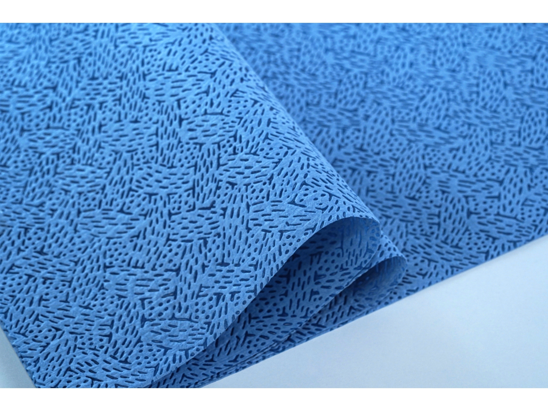
Non-woven wipes combine polyester fibers with cellulose pulp through a hydroentangling process. The result is more absorbent than pure polyester, cheaper than microfiber. Practical uses include:
- Pre-cleaning and general wipe-down—good enough for areas that don’t require better than ISO Class 6 (Class 1000) cleanliness.
- Solvent application—the absorbent structure holds solvent well for controlled wiping.
- Equipment maintenance—tough enough for machine surfaces, affordable enough to toss after a single use without feeling wasteful.
Here’s the non-negotiable: non-woven wipes are not suitable for particle-critical electronics cleanrooms. They shed significantly more fibers than knit materials and won’t meet particle generation standards for ISO Class 5 and below. If your environment involves semiconductor processing or high-density assembly, skip non-woven entirely. For a full comparison of all wipe material types, see our industrial wipes materials and types guide.
ESD-Safe Wipes: Not Optional, Mandatory
This is the section most wipe selection guides either skip or bury at the bottom. In electronics manufacturing, it’s arguably the most important factor.
Static electricity is invisible, unpredictable, and devastating to electronic components. A discharge of just 20 volts—well below what a human can feel—can damage sensitive MOSFETs, ICs, and semiconductor devices. Standard polyester wipes generate static through triboelectric charging during normal use. In an ESD-protected area (EPA), that’s a ticking time bomb.
How ESD-Safe Wipes Work
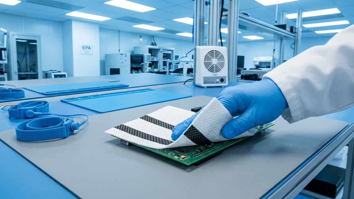
ESD-safe (anti-static) cleanroom wipes incorporate conductive fibers—typically carbon or stainless steel threads—woven into the polyester knit structure. These fibers create a controlled dissipation path that prevents static charge from building up on the wipe surface.
Key specs to look for:
- Surface resistance: 10⁶–10⁹ ohms (dissipative range). Too conductive and you risk sparking; too resistive and charge builds up anyway.
- Static decay time: Less than 0.5 seconds to dissipate 5,000V down to 50V. This is the real-world performance metric that matters.
- Charge generation: Should stay below 100 volts during normal use (per ANSI/ESD STM 37.1).
When ESD-Safe Wipes Are Non-Negotiable
- Anywhere inside a defined ESD Protected Area (EPA)
- During PCB assembly, rework, and inspection operations
- When handling bare semiconductor die, IC packages, or sensitive passive components
- Cleaning ESD-sensitive test equipment and fixtures
- Any surface that will contact unpackaged electronic components
We wrote a dedicated guide on ESD-safe industrial wipes and static damage prevention that goes deeper into the technical parameters. Worth reading alongside this article if your facility handles any ESD-sensitive components.
Matching Wipes to ISO Cleanroom Classes: Get This Wrong and You’re Wiping for Nothing
Different areas in an electronics manufacturing facility operate at very different cleanliness levels. Your SMT line might be ISO Class 7. Your wafer lithography area is ISO Class 3. Use an ISO Class 7 wipe in an ISO Class 3 environment, and you’ll exceed particle limits on the first pass. Use an ISO Class 3 wipe everywhere, and you’re burning budget for no benefit.
| ISO Class | Typical Electronics Application | Recommended Wipe Type | Particle Count (≥0.5µm/m³) |
|---|---|---|---|
| ISO 3 (Class 1) | Wafer lithography, advanced semiconductor fab | Ultra-clean polyester, pre-wetted, laser-sealed edges | ≤ 35.2 |
| ISO 4 (Class 10) | Wafer processing, photomask production | Microfiber or polyester, ultrasonic-sealed edges | ≤ 352 |
| ISO 5 (Class 100) | Semiconductor packaging, hard disk assembly | Polyester knit, sealed edges, laundered | ≤ 3,520 |
| ISO 6 (Class 1000) | SMT assembly, PCB fabrication | Polyester knit or quality non-woven, sealed edges | ≤ 35,200 |
| ISO 7 (Class 10,000) | Electronics assembly, display manufacturing | Polyester or non-woven blend, clean-cut edges | ≤ 352,000 |
| ISO 8 (Class 100,000) | General electronics, packaging areas | Non-woven blend, standard industrial grade | ≤ 3,520,000 |
The short version: match the wipe to the room. Over-spec wastes money. Under-spec risks contamination. If you’re unsure about your cleanroom classification requirements, our cleanroom dust-free cloth guide covers ISO class matching in more detail.
Edge Treatments: Laser, Ultrasonic, Cold Cut—What’s the Difference
Edge treatment is the most overlooked spec in wipe selection, and it affects performance more than most people realize. The edge is where most particle generation happens—exposed fibers at the cut boundary shed during use, contaminating the very surface you’re trying to clean.
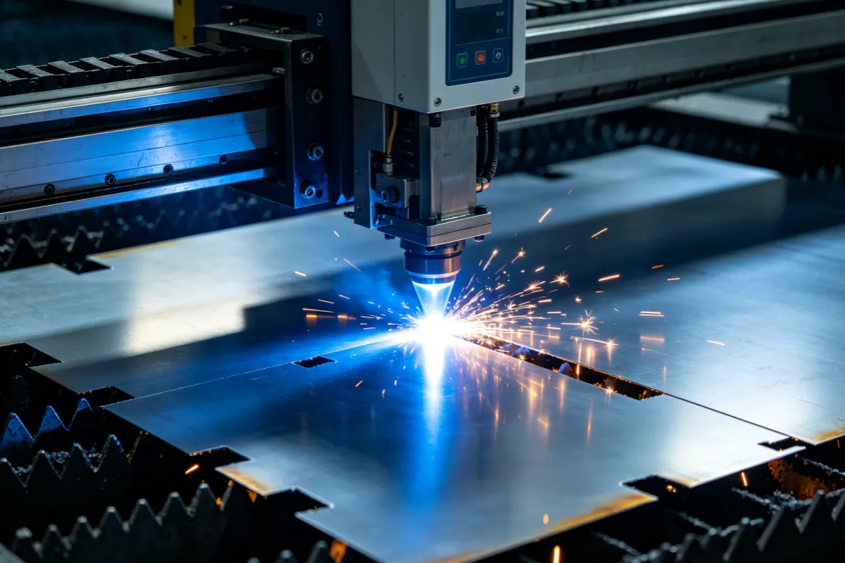
Laser-Sealed Edges
A laser melts the polyester fibers at the edge, creating a smooth, solidified border. Lowest particle generation—ideal for ISO Class 3 through 5 environments. The downside is cost and slightly stiffer edges that can leave wipe marks on very smooth surfaces.
Ultrasonic-Sealed Edges
Ultrasonic energy bonds the fibers through heat and vibration. Particle generation is slightly higher than laser sealing but still excellent for most cleanroom work. This is the sweet spot for ISO Class 5 through 7—good particle control at a more reasonable price point.
Cold-Cut Edges
A blade cuts the wipe with no heat treatment. Some cold-cut wipes use a sharp enough blade to minimize fiber disruption, but they still generate more particles than sealed options. Acceptable for ISO Class 7 through 8 and general industrial use. Not recommended for particle-critical electronics work.
Our comparison of edge sealing versus cleaning efficiency has test data if you want the full picture.
Six Real-World Application Scenarios and What to Use for Each
Enough theory. Here’s what to use where, based on actual manufacturing situations.
Scenario 1: SMT Stencil Cleaning
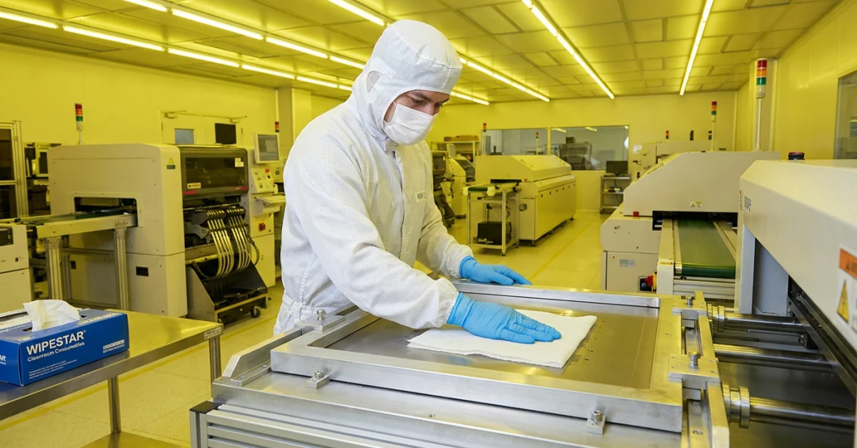
Stencil cleaning is the highest-frequency wipe operation on most SMT lines. You’re removing solder paste—fine metal alloy particles suspended in flux—from a stainless steel stencil, potentially thousands of times per shift. The wipe has to lift paste completely off aperture walls without leaving any fiber residue behind.
What to use: polyester knit wipe, pre-wetted with IPA or dedicated stencil cleaner solvent. Pre-wetting gives you even solvent distribution and eliminates the problem of pushing paste into apertures when you spray solvent onto a dry wipe on the stencil. If your stencil runs below 0.4mm pitch, insist on laser or ultrasonic sealed edges. More on this in our SMT stencil cleaning paper selection guide.
Scenario 2: Pre-Assembly PCB Cleaning
Before components are placed, bare PCBs need to be free of dust, fingerprints, and handling residue. Any particle left on a pad or in a via can cause solder defects downstream.
What to use: microfiber wipe, dry or lightly dampened with IPA. Microfiber’s particle capture ability outperforms standard polyester here because you’re dealing with a mix of contaminant types—dust, skin oils, handling debris—across a relatively large surface area.
Scenario 3: Pre-Conformal-Coating Surface Prep
Before conformal coating, the PCB surface must be spotless. Any contamination trapped under the coating creates adhesion failures, bubbles, or corrosion points. These defects often don’t show up until the product has been in the field for months, making root cause analysis expensive and painful.
What to use: lint-free polyester wipe with IPA. The surface needs to be particle-free and chemical-residue-free. Don’t use wipes with surfactants or additives—they leave invisible films that compromise coating adhesion. Our PCB assembly cleaning guide covers the full pre-coating process.
Scenario 4: ESD-Sensitive Component Handling
When handling bare ICs, MOSFETs, or other static-sensitive components, every wipe, tool, and surface in the area must be ESD-safe. No exceptions.
What to use: carbon-infused polyester wipe with verified surface resistance in the dissipative range (10⁶–10⁹ ohms) and third-party test documentation. Standard wipes—regardless of how clean they are—generate static through triboelectric charging and are not safe for these applications.
Scenario 5: Optical and Inspection Equipment
AOI cameras, solder paste inspection systems, and other optical equipment have coated lenses that scratch easily if the wipe carries abrasive particles.
What to use: soft microfiber wipe, dry or with optical-grade cleaning solution. Never use non-woven wipes on coated optics—cellulose fibers are abrasive at the microscopic level.
Scenario 6: General Cleanroom Maintenance
Wiping down benches, equipment housings, shelving, and other surfaces that don’t directly contact product.
What to use: non-woven polyester/cellulose blend with appropriate cleaning solution. Cost-effective for high-volume use where ultra-low particle generation isn’t critical. More on non-woven options in our materials guide.
Seven Specs to Verify Before You Place That Order
Before you sign that purchase order, make sure your wipe supplier can provide documentation for all seven of these specifications:
- Particle generation data—Helmke drum test (IEST-RP-CC003.4 or equivalent) results showing particles ≥ 0.5µm per square meter. For ISO Class 5 and below, demand this data. No exceptions.
- Extractable ion levels—chloride, sodium, and other ion concentrations measured via ion chromatography. High ion levels cause corrosion on copper traces and solder joints. Critical for semiconductor wafer fabrication.
- Extractable non-volatile residue (NVR)—what’s left behind after the solvent evaporates? Lower NVR means less chemical residue on your surfaces.
- Edge treatment type and verification—”sealed edges” isn’t enough. Ask for the specific method (laser, ultrasonic, heat) and test results showing particle generation from the edge itself.
- ESD properties (if applicable)—surface resistance, static decay time, and charge generation tested per ANSI/ESD standards. “Anti-static” without numbers is meaningless.
- Cleanroom-grade packaging—wipes should be double-bagged and packaged in a controlled environment. If they’re packaged in a regular factory, they’re already contaminated before you open the bag.
- Lot traceability—can the supplier trace a specific package of wipes back to the production batch, raw material lot, and QC test results? When a contamination issue hits, traceability is how you find the root cause.
If your current supplier can’t provide all seven, that’s a conversation worth having. Our cleanroom consumables supplier selection guide has a more detailed evaluation framework.
Why Electronics Manufacturers Worldwide Work With WIPESTAR
Let me be direct: WIPESTAR is not a trading company or a reseller. We manufacture cleanroom wipes and consumables from our own facility in Shenzhen, China. We control the entire production chain from raw material selection to final packaging. The reason that matters: every spec in the checklist above? We test for it ourselves, in-house, on every single batch.
The Team Behind the Product
Spec sheets get you in the door. The team behind the product is what keeps you there—especially when you’ve got a contamination mystery to solve or a custom requirement that doesn’t fit a catalog item.
- Ethan—Sales Director. 20+ years in the industrial wiping cloth and cleanroom consumables industry. He leads our global sales and has built long-term partnerships with electronics manufacturers across Asia, Europe, and North America. Complex sourcing challenges? Ethan figures out the right approach.
- Lee—Key Account Sales Manager. Joined WIPESTAR in 2018 with 7 years already under his belt in cleanroom consumables. Has worked with clients including Foxconn, Samsung, and Apple—companies where “good enough” doesn’t exist in the vocabulary. His philosophy is “Do more, know more, be more,” and he actually lives it.
- Carolina—Product Specialist. Spends her time on factory floors talking to production workers and technicians, understanding what they actually need—not what a spec sheet says they should need. She works directly with raw material suppliers to improve quality at the source.
- Guan—Cleanroom Consumables Sales Specialist. 4.5 years in semiconductors, 5+ years in cleanroom consumables. He understands the specific pain points of semiconductor, pharma, and automotive clients because he’s been solving those problems for a decade.
- Juan—Purification Industry Specialist. Deep background in clean products and purification equipment. Has been involved in the design and execution of key cleanroom projects, bringing hands-on technical experience to every customer interaction.
- Yunyun—ESD Project Manager. Specializes in ESD protection solutions for electronics manufacturing. If your facility handles sensitive semiconductors or needs to meet semiconductor contamination control standards, her team ensures you get the right ESD-safe products.
Meet the full team on our team page.
What Sets Us Apart
- We own the factory—no middlemen, no markup. Full quality control from raw material to finished product.
- OEM & ODM capability—custom sizes, fold patterns, packaging design, brand labeling, pre-saturated options. Our product range covers both standard and custom solutions.
- ISO-certified quality management—every batch tested for particle generation, extractable ions, NVR, and physical properties before release.
- ROHS compliant—meets EU hazardous substance standards. Essential if you’re exporting to European markets.
- Global logistics—regular shipments to North America, Europe, Asia-Pacific, and the Middle East with reliable, predictable lead times.
- Technical support—not sure which wipe fits your application? Our team provides recommendations based on your cleanroom class, process requirements, and budget. No charge for the consultation.
Browse our complete product catalog or contact our team for a custom recommendation.
Frequently Asked Questions
Request a Quote for Cleanroom Wipes
WIPESTAR supplies cleanroom-grade wipes direct from our factory—bulk pricing, OEM customization, fast global shipping. Every product is ISO-certified, ROHS compliant, and backed by full batch traceability documentation.