English
 Chinese

Last September I got a call from a process engineer at a logic fab in Suzhou. Their yield had been drifting down for six weeks — not crashing, just bleeding. A few hundred bad dies here, a particle excursion there. They’d recalibrated the lithography tools, swapped the photoresist batch, even brought in an outside consultant. Nothing pinned it down.
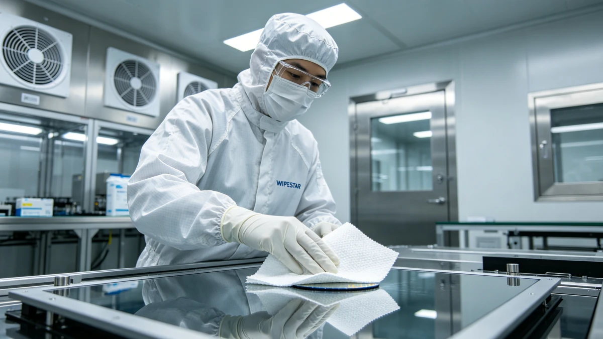
When I asked what they were using to wipe down wafer carriers between lots, the answer came back fast: “Same cloth we use in the gowning room.” That was a wood pulp/polypropylene blend — perfectly fine for mopping up spills in an ISO Class 8 corridor, absolutely wrong for an ISO Class 4 wafer handling zone. The cloth was shedding fibers under the UV inspection lamps, and those fibers were landing on wafer surfaces during transfer. Six weeks of yield loss, fixed by a wipe that cost about twelve cents more per sheet.
I’ve been in the cleanroom consumables business for over twenty years. Semiconductor fabrication is where the margin for error is thinnest — a single sub-micron particle on a 300mm wafer at a 5nm node can destroy a die worth thousands of dollars. I’ve walked through fabs in Shenzhen, Suzhou, and Hsinchu where the HVAC alone cost millions, only to watch a technician reach for a general-purpose wipe that was never meant to be inside that room.
What follows is the conversation I have with semiconductor procurement teams and process engineers every week. Not theory — the stuff that actually matters on the fab floor.
Why Semiconductor Fabs Can’t Use the Same Wipes as Everyone Else
I hear this question a lot: “A wipe is a wipe — why does semiconductor need something special?” Fair question. The honest answer is that wafer fabs operate in a contamination regime that doesn’t exist anywhere else in manufacturing.
At 7nm and below, a particle as small as 0.5µm can bridge two conductors on a wafer and kill a die. For reference, a human hair is about 70µm across. A fingerprint transfers thousands of organic molecules that can alter surface chemistry at the atomic level. The cleanroom might look spotless to the naked eye, but under the inspection tools, it’s a different story.
A pharmaceutical cleanroom running at ISO Class 7 has some breathing room. A semiconductor lithography bay at ISO Class 1 or 2 does not. The wipe you bring into that room either helps you hit your particle budget or it doesn’t — there’s no middle ground.
What Goes Wrong When You Use the Wrong Wipe
I’ve audited enough fabs to know the patterns. Here’s what I see most often:
- Fiber shedding on wafer surfaces. A general-purpose nonwoven cloth sheds fibers during normal wiping. Those fibers land on wafers and cause open circuits, bridging, or lithography defects. In a fab running 50,000 wafers a month, even a 0.1% yield hit from fiber contamination adds up to hundreds of thousands of dollars a year.
- Extractable chemicals contaminating process tools. Wipes made with binders or processing aids release trace chemicals when they contact solvents. Those extractables enter etch or deposition chambers and alter film properties — changing etch rates, introducing contamination, or creating residues on chamber walls.
- ESD-driven particle attraction. A charged wipe surface acts like a particle magnet. It pulls contaminants out of the air and deposits them on whatever it touches — creating contamination events that look random but have a systematic cause.
- Solvent breakdown leaving residue. A wipe that degrades in IPA or acetone leaves residue on the surface it’s supposed to clean. That residue interferes with photoresist adhesion, alters wet-etch uniformity, or creates defects during CMP.
Every one of these problems costs orders of magnitude more than the price difference between a cheap wipe and the right one.
Matching the Right Wipe to Each Fab Zone
Not every corner of a semiconductor fab needs the same wipe. I’ve seen facilities do both — over-specify in low-criticality zones (wasting budget) and under-specify in high-criticality zones (inviting defects). Both are expensive mistakes.
ISO Class 1–2: EUV Lithography, Extreme UV Optics
This is the tightest environment in any fab. EUV lithography systems operate in vacuum chambers with optics that are sensitive to molecular-level contamination. The wipe you use here needs verified particle counts at ≥0.1µm per lot, continuous-filament construction with no short fibers to shed, ultra-low non-volatile residue — typically under 0.01 mg/m² — and double-bagged sterile packaging that you open only inside the cleanroom. No shortcuts.
ISO Class 3: Photolithography, Ion Implant
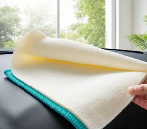
Slightly more relaxed, but still demanding. Continuous-filament polyester with sealed edges is the standard here. The W3401 Ultrasoft Surface Preparation Wipes work well in these zones — the sealed-edge construction prevents fiber shedding on photoresist-coated wafers and sensitive optical surfaces.
ISO Class 4: Etch, CVD, PVD Chamber Maintenance
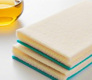
This is where the heavy contamination lives — polymer residues, recondensed materials, metal flakes from chamber components. You need a wipe that can handle scrubbing without generating the particles you’re trying to remove. The W3501 Heavy Duty Surface Preparation Wipes are built for exactly this kind of work. Tough enough for chamber cleanup, clean enough for a Class 4 environment.
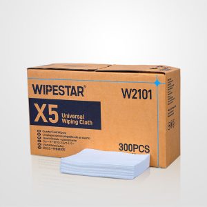
ISO Class 5: Wafer Handling, Metrology, Corridors
General cleanroom zones where the wipe still needs to be lint-free but doesn’t have to meet extreme particle specs. The W2101 Universal Wiping Cloth (X5) and W2201 Universal Wiping Cloth (X6) handle equipment exterior cleaning, spill response, and general surface wiping at a price point that makes sense for higher-volume use.
The rule is simple: match the wipe to the zone. We put together a detailed Cleanroom Wiper Selection Guide that walks through the material science behind each match. For a broader overview of wipe materials and their properties, our Industrial Wipes Materials & Types Guide covers the fundamentals.
Material Science: What Actually Works Inside a Wafer Fab
I sit down with a semiconductor client and the first question isn’t “which wipe is best?” It’s “what are you cleaning, in which zone, with what chemicals?” The answer determines everything. But here’s a breakdown of the four materials we work with most in wafer fabs:
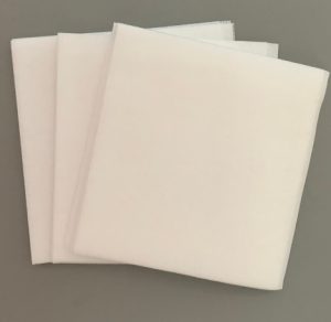
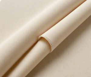
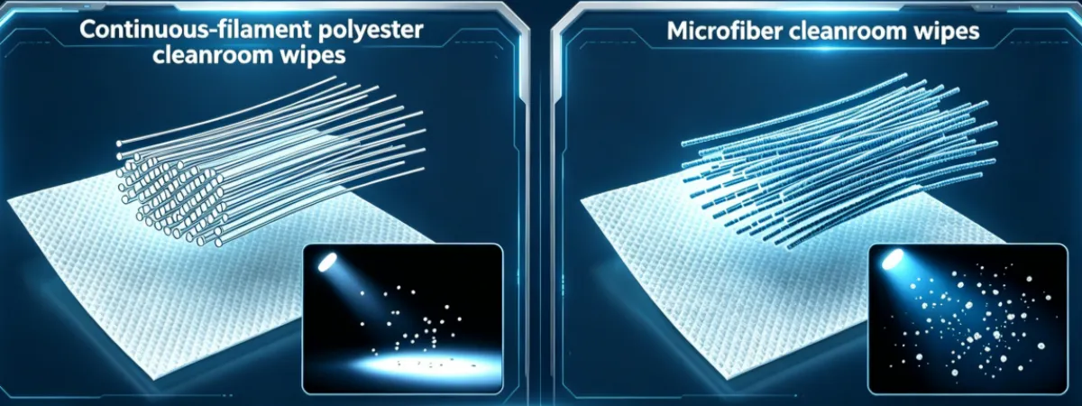
Continuous-Filament Polyester
This is what you use in the zones that matter most. The fibers are extruded as a single continuous strand — there are no short fibers to shed, even when you’re wiping a textured surface under pressure. Particle generation is the lowest of any wipe material on the market. It costs more than other options, but when a single wafer scrap can run $5,000 to $50,000, the premium on the wipe is a rounding error.
Knitted Nylon
Great abrasion resistance. If you’re cleaning etch chamber walls, shower heads, or other rough surfaces where you need some scrubbing action, knitted nylon holds up well. It pairs naturally with pre-wetted formats — our pre-wetted wipes include options validated for the solvents commonly used in semiconductor fabs.
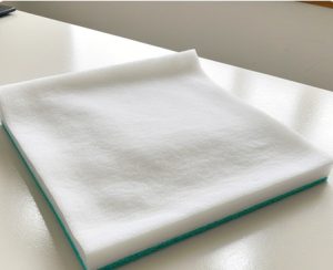
Microfiber
The split-fiber structure traps particles instead of pushing them around. That makes microfiber ideal for glass viewports, wafer inspection equipment, and polished stainless surfaces. The W5101 Microfiber Cleanroom Wiper Rolls give you cleanroom-grade microfiber in a roll format that’s convenient for high-volume use. One heads-up: microfiber doesn’t always play well with certain solvents. Test chemical compatibility before you roll it out facility-wide.
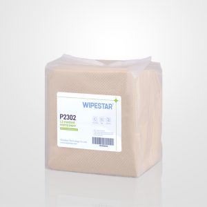
Wood Pulp / Polyester Blends
The workhorse for less critical zones — gowning rooms, corridors, packaging areas. These blends balance absorbency, strength, and cost. Don’t use them in a lithography bay. Don’t use continuous-filament polyester in a gowning room. Know the difference and you’ll save money without compromising cleanliness.
Our full wiping cloth product range covers all four material categories, each one documented with particle count data and extractable profiles.
ESD: The Contamination Problem Nobody Talks About
This one doesn’t get enough attention in semiconductor wipe discussions, and I think that’s a mistake.
Everyone knows ESD can damage sensitive devices. What fewer people realize is that electrostatic charge on a wipe surface creates a different kind of problem — it attracts and holds airborne particles. A charged wipe acts like a particle magnet. You wipe a surface, friction generates a static charge, that charge pulls contaminants out of the air, and the next surface you touch gets those contaminants deposited on it. The contamination event looks random, but the root cause is systematic.
Our ESD Project Manager Yunyun has spent years working on exactly this issue. She specializes in static control technology — research, application, and implementation — and has delivered multiple ESD projects for semiconductor clients. Her approach looks at the whole picture: the wipe material, the grounding system, the environment.
What to Look For in ESD-Safe Wipes
- Conductive fibers woven into the wipe structure — not a surface coating that wears off after a few uses
- Measured surface resistance in the 10⁶–10⁹ ohm range for semiconductor applications
- Documented static decay rate — the wipe should dissipate charge in under 0.5 seconds
- Compatibility with your existing grounding setup — wrist straps, heel straps, ESD flooring
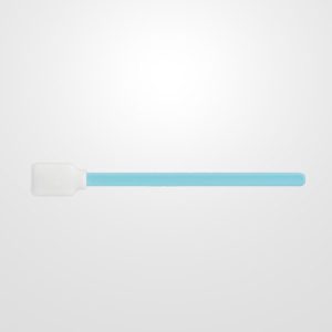
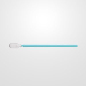
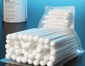
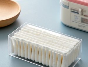
For precision cleaning in tight spots — nozzle tips, sensor housings, optical mounts — where a full-size wipe can’t reach, our cleanroom swabs come in ESD-safe configurations as well.
How We Evaluate Wipes for Semiconductor Clients
When a wafer fab contacts us — whether it’s a logic manufacturer in Shenzhen or a memory producer in Icheon — we walk through the same evaluation framework. I’ve refined this over hundreds of facility audits, and it works:
- Define the ISO zone. Where will the wipe be used? This determines acceptable particle counts, extractable limits, and packaging requirements.
- Identify the target contaminant. Photoresist residue, etch polymer, metal flakes, handling oil, general particulate — each one needs different wipe properties.
- List chemical exposures. What solvents will contact the wipe? IPA, acetone, NMP, H₂O₂, HF? Material compatibility isn’t optional.
- Confirm ESD requirements. Does the zone require ESD-safe materials? What’s the surface resistance spec?
- Review documentation needs. COA with particle count data, ROHS compliance, NVR/FTIR/IC test results — whatever your quality system requires.
- Request samples and test on-site. We don’t push bulk orders without trials. Send us your specs, we’ll send you samples from our product catalog. Test them in your environment, under your conditions.
For a detailed breakdown of material properties by application, our Wiping Cloth Selection Guide is a good starting point.
The Real Math: What Cheap Wipes Actually Cost
I had a procurement manager tell me once that his fab saved $30,000 a year by switching to a cheaper wipe supplier. I asked him what his yield loss was for the same period. He pulled up the data — $380,000 in scrap and rework, up from $90,000 the year before. He saved $30,000 on wipes and lost $290,000 on yield. That’s not a bargain.
Here’s a more realistic breakdown for a typical 300mm logic fab:
| Scenario | Yield Loss | Annual Scrap Cost | Wipe Spend | Total Cost |
|---|---|---|---|---|
| General-purpose nonwoven wipes | 0.5–1.0% | $250,000–$500,000 | $15,000 | $265,000–$515,000 |
| Semiconductor-grade wipes | <0.1% | <$50,000 | $45,000 | <$95,000 |
The semiconductor-grade wipe costs roughly 3× more per sheet. It saves 80% or more in total contamination cost. I wrote about this dynamic in more detail in our article on industrial cleaning wipes and total cost of ownership — the semiconductor case is the most extreme version of the principle. For broader procurement strategies, our guide on reducing industrial wiping cloth costs applies to wafer fabs as much as anywhere else.
Our Team — And Why That Matters
I’ll be straightforward about this: when you’re trusting someone with your contamination control strategy, you want to know who you’re talking to. Product specs matter, but the people behind the product matter just as much — especially when you’ve got a tricky application or a process that’s giving you grief.
Ethan, our Sales Director, has been in the industrial wiping cloth and cleanroom consumables industry for over 20 years. He’s led our team through hundreds of semiconductor facility audits. If you’ve got a complex requirement — a new process, a zone transition, an unusual contaminant — Ethan’s the one who figures out the right approach.
Guan spent 4.5 years in the semiconductor industry before joining us, plus another 5+ years in cleanroom consumables sales. He gets the specific pain points of wafer fab clients because he’s been solving those problems for years. Semiconductor, pharmaceutical, automotive — he’s worked across all of them.
Lee joined us in 2018 and manages key accounts including clients like Foxconn, Samsung, and Apple — companies that don’t tolerate “good enough.” His philosophy is “Do more, know more, be more,” and honestly, he lives it.
Yunyun is our ESD Project Manager — dedicated to static control technology with deep experience in research, application, and solution implementation. She’s delivered multiple ESD projects for semiconductor environments and brings a contamination perspective that most wipe suppliers simply don’t have on staff.
Juan is our Purification Industry Specialist with a background in cleanroom design and purification process equipment. When a semiconductor client needs to integrate wipe selection into a broader contamination control strategy — HVAC, gowning protocols, environmental monitoring — Juan connects those dots.
Carolina is our Product Specialist. She’s the one on the factory floor talking to the production workers and technicians, understanding what they actually need versus what a spec sheet says they should need. That real-world feedback drives our product development.
Meet the full WIPESTAR team.
OEM, Custom Work, and Getting Started
We’re not a trading company. We manufacture cleanroom consumables from our own facility in Shenzhen — over 100,000 square meters of production space, 1,200+ specialized machines, cleanroom workshops running at ISO Class 4 through ISO Class 7. Every batch ships with full traceability: COAs, particle count data, ROHS compliance.
Need a specific size for your wafer carrier? Custom saturation levels for pre-wetted wipes? Private-label packaging? We handle OEM and ODM orders at scale, with stable lead times and competitive factory-direct pricing.
Browse the complete WIPESTAR product range, or contact our team directly at info@wipestar.com or +86-755-8961-6775 for application-specific recommendations.
WIPESTAR — Making the World Cleaner.
Frequently Asked Questions
Request a Quote for Semiconductor Cleanroom Consumables
We supply semiconductor-grade cleanroom wipes, ESD-safe wipers, surface preparation wipes, and cleanroom swabs direct from our factory — bulk pricing, OEM customization, fast global shipping. Everything is ISO-certified and ROHS compliant.