English
 Chinese

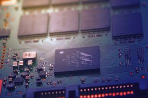
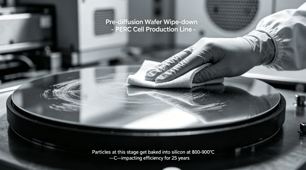
A PERC cell manufacturer in Anhui was chasing a 0.3% absolute efficiency gap between their best and worst production lots. They’d optimized their texturing bath, tightened their diffusion furnace temperature control, and refined their PECVD anti-reflection coating parameters. The gap narrowed to 0.15%. Then their process engineer noticed something: the efficiency distribution correlated with which shift was running the line. Not because of operator skill—because of which wiping cloth each shift used for the pre-diffusion wafer wipe-down. One shift had switched to a cheaper wipe three months earlier without telling anyone.
We supply cleanroom consumables to solar cell manufacturers, module assembly lines, and PV equipment OEMs across Asia. This is what we’ve learned about matching wipes to photovoltaic manufacturing—where a particle on a wafer surface doesn’t just cause a defect, it permanently reduces the power output of every cell that passes through that station.
Why Solar Cell Manufacturing Has Unique Contamination Challenges
Solar cell manufacturing sits at the intersection of semiconductor-grade surface sensitivity and high-volume production speed. A typical cell line processes 3,000–6,000 wafers per hour. At that throughput, every second of wipe-down time per wafer translates to real capacity loss—and every particle that survives the wipe becomes a permanent efficiency reduction.
The contamination chain in PV manufacturing is different from semiconductor or display manufacturing in three ways:
- Efficiency, not yield, is the metric — In semiconductor fab, a particle causes a die failure and the die is scrapped. In solar cell manufacturing, a particle on the wafer surface causes a local shunt or recombination site that reduces cell efficiency by 0.1–0.5%. The cell still works—it just produces less power. Over a 25-year module lifetime, that 0.3% efficiency loss per cell adds up to significant energy yield reduction for the end customer.
- Wafer fragility — Mono PERC and HJT wafers are 150–170μm thick—thin enough to flex and crack during handling. Your wipe must not apply uneven pressure that bends the wafer during wipe-down. A cracked wafer is a complete scrap loss; a contaminated wafer is just an efficiency loss.
- Chemical process environment — PV manufacturing uses aggressive chemicals (HF, KOH, HNO₃, POCl₃) at high temperatures and concentrations. Your wipe must be compatible with these chemicals and must not introduce contaminants that affect chemical bath life or process uniformity.
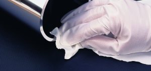
Silicon Wafer Handling: The Wipe That Touches Your Product
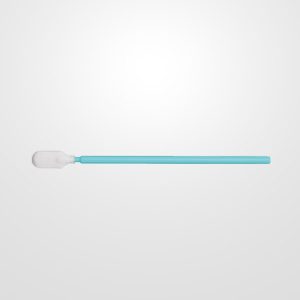
In most solar cell production lines, there’s at least one wipe-down step where a wiping cloth contacts the bare silicon wafer surface. This is the highest-risk contamination point in your process, and the wipe specification here directly determines your cell efficiency distribution.
Pre-Texture Wipe-Down
After wafer slicing and cleaning, some manufacturers wipe the wafer surface to remove residual slurry particles from the wire saw process. The wipe must be:
- Ultra-low-lint—any fiber on the wafer surface becomes a masking site during texturing, creating an untextured patch that reflects light instead of absorbing it.
- Soft enough not to micro-scratch the silicon surface—scratches on the wafer surface become recombination sites that reduce minority carrier lifetime.
- Free of metallic contamination—transition metals (Fe, Cu, Cr, Ni) on the wafer surface diffuse into silicon during the high-temperature diffusion step and create recombination centers that permanently reduce cell efficiency.
Pre-Diffusion Wipe-Down
This is the wipe step that caught the Anhui manufacturer. After texturing and cleaning, the wafer surface must be particle-free before entering the diffusion furnace. Any particle on the surface at this point gets baked into the silicon during the 800–900°C diffusion process and becomes a permanent defect. The wipe must remove particles without introducing fibers, metallic contamination, or organic residue that affects POCl₃ diffusion uniformity.
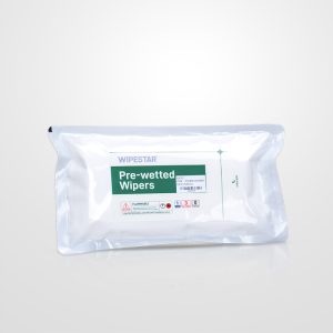
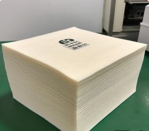
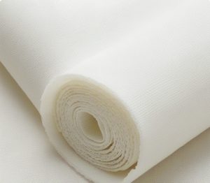
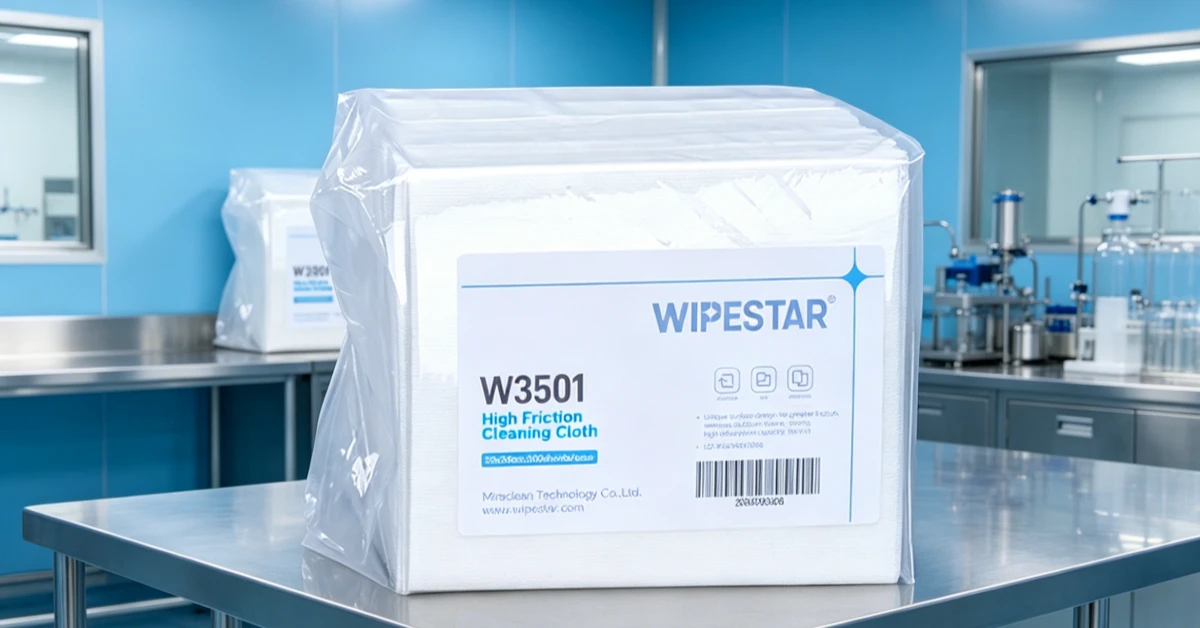
We recommend a 100% polyester, laser-sealed wipe manufactured in ISO Class 5 conditions for pre-diffusion wipe-down. The polyester provides chemical resistance to the trace HF residue on the wafer surface. The laser-sealed edge eliminates fiber shedding. The ISO Class 5 manufacturing environment minimizes embedded particles.
Texturing and Etching: Wipe Selection for Wet Chemical Processes
Solar cell texturing—KOH-based random pyramid texturing for mono-Si, or acid-based texturing for multi-Si—creates the surface structure that traps light and reduces reflection. The chemical baths, transfer rollers, and tank interiors all require periodic wipe-down with chemically compatible materials.
KOH Texturing Bath Maintenance
Potassium hydroxide texturing baths operate at 80–90°C with KOH concentrations of 2–5% by weight. Wipe-down of tank rims, transfer rollers, and bath maintenance equipment requires wipes that withstand strong alkaline conditions at elevated temperatures. Cellulose-based wipes degrade in hot KOH—use polypropylene or polyester wipes that maintain physical integrity in alkaline environments.
HF and HNO₃ Etching
Isotropic etching with HF/HNO₃ mixtures is used for saw damage removal and surface cleaning. HF attacks glass-based materials and some polymers—your wipe must be HF-compatible. Polypropylene is the safest choice for HF-contact applications. Polyester is acceptable for dilute HF but degrades in concentrated solutions. Never use cellulose or glass-fiber wipes near HF—they dissolve and contaminate the bath.
Bath Life Extension
Contamination from wipes and other consumables is a leading cause of premature chemical bath exhaustion. Particles, fibers, and chemical extractables from the wipe accumulate in the bath and affect texturing uniformity. Using a cleaner wipe extends your bath life and reduces chemical consumption. One PV manufacturer we work with extended their KOH bath life by 15% simply by switching to a lower-extractable wipe for tank rim cleaning—the wipe cost increase was offset three times over by the chemical savings.
Diffusion and PECVD: Pre-Process Surface Preparation
Before diffusion (POCl₃ doping) and PECVD (anti-reflection coating deposition), equipment interiors require wipe-down to remove phosphorus glass buildup, silicon nitride residue, and particulate contamination from previous runs.
Diffusion Furnace Tube Cleaning
Phosphorus oxychloride (POCl₃) diffusion deposits a phosphosilicate glass (PSG) layer on furnace tube walls, quartz boats, and wafer handling fixtures. Periodic cleaning removes this buildup to prevent particle generation and cross-contamination between batches. The wipe must be compatible with the HF-based cleaning solution used to dissolve PSG—polypropylene or polyester with verified HF resistance.
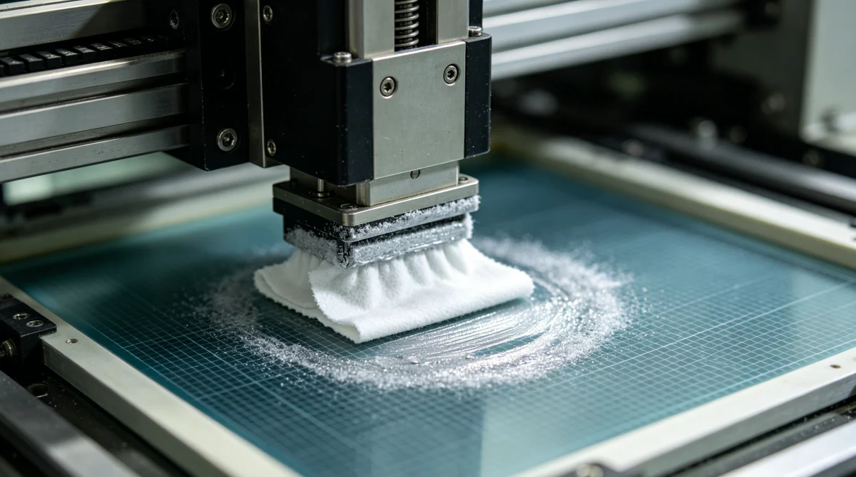
PECVD Chamber Cleaning
PECVD (Plasma-Enhanced Chemical Vapor Deposition) chambers deposit silicon nitride anti-reflection coatings. Chamber walls accumulate silicon nitride deposits that flake off and contaminate wafers during subsequent runs. Chamber wipe-down between maintenance cycles requires wipes that remove hard deposits without generating fibers that contaminate the chamber. A heavy-duty polyester wipe with high abrasion resistance works well for PECVD chamber cleaning—the mechanical action removes deposited films without tearing.
Wafer Carrier and Boat Cleaning
Quartz wafer carriers and silicon carbide boats accumulate residue from repeated high-temperature processing. Cleaning these fixtures requires wipes compatible with the specific residue chemistry. For PSG-coated quartz, use an HF-compatible wipe. For silicon carbide boats with silicon nitride residue, use an abrasive polyester wipe that can dislodge the deposited film without scratching the boat surface.
Metallization and Firing: Post-Processing Surface Cleaning
After diffusion, PECVD, and passivation, the cell enters metallization—screen printing of silver and aluminum paste contacts, followed by a co-firing step at 800–900°C. Post-metallization cleaning is the last wipe-down before cell testing and sorting.
Screen Print Station Cleaning
Silver and aluminum paste are viscous, sticky materials that contaminate everything they touch. Wipe-down of screen print heads, squeegees, and paste reservoirs between print runs requires a wipe with high absorption capacity and mechanical strength. The wipe must absorb the organic vehicle from the paste without leaving fibers that clog the screen mesh. A medium-weight cellulose/polyester blend with sealed edges works for paste cleanup—the cellulose absorbs the organic vehicle, and the polyester adds wet strength.
Post-Fire Surface Cleaning
After co-firing, the cell surface may have fired-on residue from the belt furnace—belt fiber fragments, flux residue, and glass frit particles. This residue affects cell appearance and can cause hot spots if it creates localized shunting paths. A soft, low-abrasion wipe with IPA removes fired-on residue without scratching the contact fingers or anti-reflection coating.
Cell Testing and Sorting
Before IV testing, the cell surface should be clean and fingerprint-free. Handling marks and residual paste affect the anti-reflection coating’s light-trapping performance and can cause measurement variability. A final wipe-down with a soft, lint-free wipe ensures consistent test results across the production run.
Module Assembly: Lamination, Stringing, and Junction Box Cleaning
After cell testing and sorting, cells are assembled into modules through stringing, lamination, framing, and junction box installation. Each step has its own wipe requirements.
Cell Stringing
Cell stringing uses solder ribbon to connect cells in series. The soldering surface must be free of oxidation, flux residue, and finger contamination. Wipe-down of soldering iron tips and ribbon guides with a flux-compatible wipe ensures consistent solder joint quality. A cold joint from a contaminated soldering surface is a module failure that shows up in the field 2–3 years after installation.
Pre-Lamination Cleaning
Before lamination, the cell string and EVA (ethylene-vinyl acetate) encapsulant surface must be free of particles, fibers, and finger marks. Any particle trapped between the cell and EVA becomes a delamination nucleation site under thermal cycling—a defect that grows over the module’s 25-year lifetime. Use a lint-free, anti-static wipe for pre-lamination cleaning. The anti-static property prevents the EVA film from attracting airborne particles during handling.
Junction Box Installation
Junction box potting and cable termination require surfaces free of silicone, oil, and moisture. The wipe must remove handling contamination without leaving residue that affects potting compound adhesion. A silicone-free wipe is mandatory—silicone contamination prevents potting compound from bonding to the junction box housing, causing moisture ingress and connector corrosion in the field.
ESD and Anti-Static Requirements in PV Manufacturing
Electrostatic discharge is a growing concern in solar cell manufacturing as cell architectures become more complex. PERC, HJT, and TOPCon cells all have thin dielectric layers that are sensitive to static-induced damage.
- PERC cells — The rear Al₂O₃/SiNₓ passivation stack is 10–30nm thick. Static discharge through this layer creates a local shunt path that reduces cell efficiency. Anti-static wipes for PERC rear-side handling prevent static-induced shunt formation.
- HJT cells — Heterojunction technology uses ultra-thin amorphous silicon layers (5–10nm) that are highly sensitive to both static discharge and contamination. HJT cell handling requires the cleanest, most ESD-safe consumables available.
- TOPCon cells — Tunnel oxide passivated contacts use a 1–2nm SiO₂ tunneling layer. Static damage to this layer is catastrophic for cell performance. ESD-safe handling and wipe-down procedures are critical for TOPCon production.
For all advanced cell architectures, specify wipes with surface resistivity in the dissipative range (10⁶–10¹¹ ohms/square) for all wafer and cell handling applications. Standard wipes in standard cleanroom conditions generate enough static to damage these thin dielectric layers.
Your PV Consumables Team at WIPESTAR
Solar manufacturing accounts get a team that understands PV process chemistry and the economics of cell efficiency—not generalists selling the same wipe to every industry.

Lee — Key Account Sales Manager
Lee manages major PV manufacturer accounts with the volume planning that gigawatt-scale production demands. Solar cell lines run 24/7 and consume wipes at a rate that requires tight supply chain coordination. He handles multi-line supply agreements, manages safety stock programs, and coordinates with your procurement team to align delivery schedules with production ramp plans.

Juan — Purification Industry Specialist
Juan’s contamination control background covers wet chemical processes—the KOH texturing baths, HF etch tanks, and POCl₃ diffusion furnaces that define PV cell manufacturing. He understands how wipe extractables affect chemical bath life, how particle contamination affects cell efficiency, and how to match wipe specifications to each process step in the cell line.

Guan — Cleanroom Consumables Sales Specialist
Guan handles cleanroom consumable applications for PV manufacturers—from wafer handling wipes to module assembly consumables. He coordinates product trials, manages qualification documentation, and tracks lot-level quality data for solar customers. He’s the one who runs the wipe comparison trials that show you the efficiency difference between your current wipe and the optimized specification.

Daisy — Sales Support
Daisy handles sample coordination and documentation packages for PV manufacturers evaluating new wipe products. She assembles the qualification data—particle counts, extractable metal reports, chemical compatibility certificates—and gets it to your process engineering team on schedule. For high-volume solar accounts, she manages the ongoing documentation updates that keep your approved supplier list current.
Meet the full team: WIPESTAR Team Page →
Frequently Asked Questions About Cleanroom Wipes for Solar Panel Manufacturing
Request Solar Manufacturing Wipe Samples
We supply cleanroom wipes for solar panel photovoltaic cell manufacturing—metal-scanned wafer handling wipes, HF-compatible chemical process wipes, anti-static cell handling consumables, and paste cleanup wipes for metallization. ISO 9001:2015 certified production. Free samples with extractable data for qualified PV manufacturers.
Browse our cleanroom wipe range →
Request PV Manufacturing Samples →